What is Thin Film Deposition?
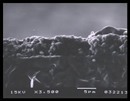
Thin film deposition techniques are used to produce material ranging from single-atom-thick monolayers up to layers several micrometers in thickness. These techniques are used to produce wear-resistant surfaces, optical coatings, and semiconductor devices. Thin film deposition techniques can typically be classified as physical or chemical.
#11: American Elements Assists Teledyne in Creation of New Light Absorbing Coating
In physical deposition methods, the source material often has the same chemical composition as the desired thin film, and is merely being transferred through mechanical or thermodynamic means from the bulk source material to the substrate surface. Alternately, a compound thin-film can be produced with physical techniques through deposition of alternating layers of elemental source materials, deposition in the presence of a reactive gas, or co-deposition of two materials. The source materials used in physical deposition techniques are single-element or compound sputtering targets, bulk evaporative metals or compounds in the form of pellets, powders, or wire, and reactive gases.
In chemical deposition methods, the elements to be deposited are present as components of precursor compounds, and a chemical process occurs at the substrate surface to produce the desired thin film material. The source materials used in chemical deposition methods include bulk forms of pure elements, reactive gases, organometallic compounds, metal salts, metal halides, and metal hydrides.
Some thin films are produced almost exclusively by a single technique, but many have several potential fabrication routes. For instance, nitrides may be deposited using traditional sputtering from a nitride target, reactive sputtering using a pure metal target in the presence of nitrogen gas, or a variety of chemical deposition methods dependent on the other element.
Deposition Techniques
Physical Deposition Techniques
Electron beam physical vapor deposition (EBPVD)
Electron beam physical vapor deposition (EBPVD) is a form of physical vapor deposition in which the target is vaporized as a result of bombardment with an electron beam under high vacuum. This technique can provide a higher deposition rate than most physical deposition processes, and uses source material more efficiently than other methods. The primary disadvantage of EBPVD is that it is not compatible with all film materials or substrates. The high temperatures required for vaporization causes fragmentation of many compounds; this leads to deposition of films with substantially altered stoichiometry compared to the source material. In some cases this problem can be overcome through co-evaporation of the component elements at precisely controlled rates, but some materials are entirely incompatible with EBPVD.
Molecular beam epitaxy (MBE)
Molecular beam epitaxy (MBE) is an evaporative physical deposition technique that utilizes a low deposition rate and ultra-high vacuum to produce thin films with precisely controlled composition and structure. Each component element of the desired thin film composition is present as a separate source material whose release can be individually controlled by opening and closing shutters on the individual effusion cell containing the element. This precise control allows thickness of the film to be controlled down to a single layer of atoms, and allows production of intricate structures containing layers of different materials or special features such as quantum wells or quantum dots. MBE is also the only physical deposition technique used to produce single-crystal thin films. This technique is primarily used in applications requiring an extremely high degree of precision, most often related to the fabrication of semiconductor devices.
Sputtering Deposition
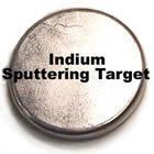
Sputtering deposition is a process in which atoms are ejected from a solid target material due to bombardment of the target with extremely high energy particles, which may be a plasma, an ion source, a particle accelerator, or a radioactive material that emits alpha particles. The ejected atoms are then deposited on the substrate surface. Traditional sputtering deposition occurs in a vacuum and uses an inert gas for high-energy particle bombardment, and thus the source material, which comes in the form of a sputtering target, has the same chemical composition as the intended thin film. In reactive sputtering, a reactive gas such as nitrogen or oxygen is introduced into the chamber, and reacts with the sputtered element to produce a compound film; this process is sometimes used to produce compound films such as oxides and nitrides using single-element sputtering targets. Sputtering has an advantage over other physical deposition methods in that it does not require high temperatures, and even materials with extraordinarily high melting points can be deposited using sputtering techniques. Disadvantages of the technique include incompatibility with some methods of patterning/structuring thin films, and the likelihood of some degree of contamination of the thin films with the inert sputtering gases. The compatibility of sputtering deposition with a wide range of materials including metals, nitrides, oxides, and some compound semiconductors has lead to its widespread use in integrated circuit fabrication, tool bit and glass coating, and optical disk manufacturing.
For more information on sputtering deposition and to view American Elements catalog of sputtering target products, please click here: Sputtering Targets
Pulsed Laser Deposition (PLD)
Pulsed laser deposition (PLD) is a flexible physical deposition technique that uses laser pulses to produce a plasma that is then deposited in on the substrate. This method can be used in environments ranging from high vacuum to atmospheric pressures, is compatible with the use of reactive gases, and can be used with almost any material. The primary advantage of this method is the ability to preserve stoichiometry of very complex materials, including the complex oxide functional materials used as high temperature superconductors, ferroelectric films, and high tech sensors. A potential problem with this technique is the presence of micron-sized particulates and poor uniformity of films deposited over large surface areas, but these problems are becoming less relevant as PLD technology continues to improve.
Cathodic Arc Deposition (arc-PVD)
Cathodic arc deposition (arc-PVD) is a physical vapor deposition technique that uses an electric arc to vaporize the source material. It is notable for being a particularly cost effective vacuum deposition technique, but is limited in the range of materials it can be used with. Most frequently, arc-PVD is used to produce hard and low-friction nitride or diamond-like carbon coatings on tools, machine components, and decorative items.
Chemical Deposition Techniques
Plating
Plating is a method for depositing metal films from aqueous solution. In electroplating, the process is driven by an electrical current, while in electroless plating, the process is an autocatalytic redox reaction. Plating can be used to produce thick films as well as thin films, and historically has been used for decoration, corrosion and wear inhibition, and to alter surface properties of metal objects. In electronics manufacturing, plating techniques are frequently used to deposit gold or silver for electrical connectors.
Sol-Gel Deposition
Sol-gel deposition describes the production of solid thin thin films from liquid solutions through the gradual removal of the liquid solvent. Typically the dissolved precursors are metal alkoxides and/or metal chlorides, the solvent is an organic liquid, and the thin film produced is a metal oxide. A uniform thin film may be achieved by dipping the substrate in the solution and allowing it to dry (dip coating), or by applying the solution to the center of the substrate and then spinning the substrate at high speeds until the coating has reached the desired thickness (spin coating). Sol-gel deposition is notable as a relatively cheap and low-temperature thin film technique that allows fine control of final chemical composition.
Chemical Vapor Deposition (CVD)
Chemical vapor deposition (CVD) refers to a range of chemical deposition processes in which one or more gas-phase precursors react or decompose at a substrate surface, forming a thin film. A variety material types can be produced with these techniques, including monocrystalline, polycrystalline, amorphous, and nanostructured materials. Some particularly common and industrially important CVD processes include the deposition of polycrystalline silicon and silicon dioxide from silane precursors, deposition of silicon nitride from the reaction of silane and ammonia, deposition of tungsten from tungsten hexafluoride, and of molybdenum, tantalum, titanium, and nickel from their respective chlorides, and low-pressure growth of synthetic diamond. Some notable variants of CVD are discussed below.
Metalorganic Vapor Phase Epitaxy (MOVPE)
Metalorganic vapor phase epitaxy (MOVPE) is a CVD method used to produce single crystal or polycrystalline thin films of semiconductor materials. High temperatures in the reaction chamber lead to pyrolytic decomposition of the precursor compounds-- typically alkylated metals and reactive hydride gases (arsine, phosphine, or ammonia)--and the film compound then forms on the surface of the substrate wafer.
Plasma-Enhanced Chemical Vapor Deposition (PECVD)
Plasma-enhanced chemical vapor deposition (PECVD) is a CVD method in which an electrical discharge between two electrodes is used to ionize the reacting gases, allowing for fast deposition at lower temperatures than possible with most other vapor deposition techniques. This method is typically used in semiconductor manufacturing to deposit films onto wafers containing temperature-sensitive structures.
Hydride Vapour Phase Epitaxy (HVPE)
Hydride Vapour Phase Epitaxy (HVPE) is an epitaxial CVD technique employed to produce III-V semiconductors and alloys of those compounds. In this method, hydrogen chloride is reacted with group-III metals to produce gaseous metal chlorides, which then react with ammonia, phosphine, or arsine gas to produce nitrides, phosphides, or arsenides respectively. This method has a substantially higher growth rate than other methods available to produce these materials, yet still produces high-quality materials with few impurities and efficient doping. Materials produced using HVPE are particularly important for production of GaN-based blue, green, and white LEDs and blue laser diodes.
Hybrid Physical Chemical Vapor Deposition (HPCVD)
Though several techniques discussed previously could arguably be considered both chemical and physical deposition processes--notably, the use of physical techniques like sputtering in the presence of reactive gases--HPCVD refers specifically to deposition processes involving the heat-induced chemical decomposition of a precursor gas and the thermal evaporation of a bulk metal. Most frequently, HPCVD is used to deposit magnesium diboride films, as alternate methods for deposition of this compound typically produce rough and non-stoichiometric thin films.
Atomic Layer Deposition (ALD)
Atomic layer deposition (ALD) is a CVD process in which the film is grown one single atomic layer at a time. In compound films, this is accomplished by sequential, alternating exposures of precursor compounds to the substrate, with purges of the reaction chamber in between exposures. In single element films, a treatment such as plasma exposure must be applied following each deposition of an atomic layer in order to reactivate the surface for further deposition. Thickness of films deposited by ALD is therefore precisely controlled by the number of deposition/purge cycles. This method allows precise control of composition and structure, and allows straightforward growth of multilayer structures, but is relatively slow related to comparable techniques and cannot be used to deposit all important microelectronics materials. ALD is most often used to deposit gate oxides, transition metal nitrides used as both barrier metals and gate metals, and metal electrodes and interconnects.
Thin Film Applications
Electronics and Semiconductors
Integrated circuit fabrication
The incredibly complex structures that make up the integrated circuits found in almost all electronic devices are patterned using a series of thin film deposition techniques in combination with etching and patterning technologies. Materials used include both elemental and compound semiconductors, gate oxides, metal interconnects, and protective/insulating coatings.
-
Thin-film batteries
Thin-film batteries are made using conventional battery materials, but are constructed using thin films to produce lighter, more compact, and even flexible batteries. A variety of thin film deposition methods are used to produce the various battery components.
-
Thin-film solar cells
Thin-film solar cells composed of materials such as copper indium gallium selenide (CIGS), cadmium telluride (CdTe), and amorphous silicon (a-Si) are cheaper alternatives to bulk crystalline silicon-based solar cell technologies.
-
Transparent conducting films
Optically transparent electrical conductors are essential for common optoelectronic devices such as displays, photovoltaics, and LEDs. The most widely used of these materials is tin-doped indium oxide (ITO). The rising demand for electronic displays in combination with indium’s scarcity has lead to high prices for ITO, and alternative conductive metal oxides such as aluminum-doped zinc oxide (AZO) are sometimes used instead. Additionally, transparent conductive polymers are used in organic electronics. Transparent conductive oxides (TCOs) can be deposited using a variety of deposition techniques, while transparent conducting polymers are produced using sol-gel methods.
-
Phase change alloys
Phase change alloys such as germanium antimony tellurium (GeSbTe or GST) can take either a crystalline or amorphous structure depending on the conditions under which they are formed, a property which is exploited to product phase change based computer memory devices. These materials are deposited using metal organic chemical vapor deposition (MOCVD).
-
Optical data storage
Optical discs such as CDs and DVDs are produced using thin film deposition techniques. Recording layers of masters and of recordable or rewritable discs may be deposited using a variety of methods depending on the type of disc being produced, while the reflective metal layer is typically produced through sputtering.
Wear-resistant coatings
Thin film deposition techniques can be used to deposit materials that resist damage from heat, corrosion, and mechanical wear. Wear-resistant coatings are frequently used to extend the life of cutting tools, engine parts, and other components exposed to extreme environments. High performance ceramic materials such as carbides and nitrides are frequently used for these types of applications.
Optical coatings
Optical coatings are applied to architectural glass or optical components in order to alter transmission of electromagnetic waves through the material. Metal films are frequently deposited on glass in order to produce mirrors, while magnesium fluoride, calcium fluoride, and various metal oxides are used to tailor the precise reflective properties of a material, producing anti-reflection or high-reflection surfaces. Additionally, titanium dioxide-based surface coatings may be deposited on lenses and windows to produce self-cleaning surfaces.
Packaging materials
Thin film techniques are used to produce metalized films: polymer films coated with a thin layer of metal, usually aluminum. These films are used decoratively, in food packaging, in insulation materials, and in specialty electronics applications.
Solid Oxide Fuel Cells
 Typical solid oxide fuel cell (SOFC) designs contain an electronically conductive low density cathode, a high density, ionically conductive electrolyte, and an electronically conductive open air electrode. Sputtering targets are produced by American Elements to meet the needs of each of these layers. Our offerings include perovskite cathode materials such as Lanthanum Strontium Manganite (LSM), Lanthanum Strontium Ferrite (LSF), Lanthanum Strontium Cobaltite Ferrite (LSCF), Lanthanum Strontium Chromite (LSC), and Lanthanum Strontium Gallate Magnesite (LSGM) with doping levels and other parameters to customer specifications, as well as ion-conducting electrolyte materials such as YSZ (Yttria stabilized Zirconia), SCZ (Scandium doped Zirconia), Samarium doped Ceria, Gadolinium doped Ceria and Yttrium doped Ceria. These fuel cells materials are marketed under the trademark AE Fuel Cells™.
Below is only a limited selection of the full catalog of thin film deposition and evaporation products that American Elements manufactures. If you do not see a material you're looking for listed, please search the website or contact customerservice@americanelements.com.
American Elements manufactures a comprehensive array of materials for thin film deposition, including evaporation materials, organometallic precursors, and sputtering targets. We offer evaporation materials such as pure metals, oxides, fluorides, alloys, and other compounds in the forms of pellets, pieces, powders, wires, rods, ingots, chunks, shot, tablets, and many others.
American Elements casts any of the rare earth metals and most other advanced material into rod, bar or plate form, as well as other machined shapes. All as-cast rods, bars and plates are produced from either the pure metal ingots or sublimed metals. We have a variety of standard sized rod molds, from a minimum of 1/4" diameter up to 3" diameter for most rod needs. Plates are also offered in standard thicknesses, from 1/4" thick to 1" thick. Maximum rod lengths and maximum plate sizes are dependent on melt capacity and furnace room. Small diameter rods may have only a 4"-6" maximum cast length, whereas larger diameter rods may be cast up to about 16" long. Plate sizes can be cast up to a size of 24" x 16". As-cast rods or plates are saw-cut to length or final dimensions, and the metal surface may have visible flow marks.
Above is a select offering of our thin film materials catalog; for forms and materials not included in this, you may visit our Metals, Alloys, or Organometallics product catalogs; you may also request a quote directly for a material. We custom manufacture all materials to customer specifications for shape, size, purity, composition in all amounts including bulk quantities.
For the American Elements catalog of Sputtering Target products, please click here.