SECTION 1. IDENTIFICATION
Product Name: Gallium Arsenide
Product Number: All applicable American Elements product codes, e.g. GA-AS-05-I
, GA-AS-05-L
, GA-AS-05-P
, GA-AS-05-ST
, GA-AS-05-WF
CAS #: 1303-00-0
Relevant identified uses of the substance: Scientific research and development
Supplier details:
American Elements
10884 Weyburn Ave.
Los Angeles, CA 90024
Tel: +1 310-208-0551
Fax: +1 310-208-0351
Emergency telephone number:
Domestic, North America: +1 800-424-9300
International: +1 703-527-3887
SECTION 2. HAZARDS IDENTIFICATION
Classification of the substance or mixture
Classification according to Regulation (EC) No 1272/2008
GHS06 Skull and crossbones
Acute Tox. 3 H301 Toxic if swallowed.
Acute Tox. 3 H331 Toxic if inhaled.
Classification according to Directive 67/548/EEC or Directive 1999/45/EC
T; Toxic
R23/25: Toxic by inhalation and if swallowed.
N; Dangerous for the environment
R50/53: Very toxic to aquatic organisms, may cause long-term adverse effects in the aquatic environment.
Information concerning particular hazards for human and environment:
N/A
Hazards not otherwise classified
No data available
Label elements
Labelling according to Regulation (EC) No 1272/2008
The substance is classified and labeled according to the CLP regulation.
Hazard pictograms

GHS06
Signal word
Danger
Hazard statements
H301+H331 Toxic if swallowed or if inhaled.
Precautionary statements
P261 Avoid breathing dust/fume/gas/mist/vapors/spray.
P301+P310 IF SWALLOWED: Immediately call a POISON CENTER/ doctor/...
P304+P340 IF INHALED: Remove person to fresh air and keep comfortable for breathing.
P311 Call a POISON CENTER/doctor/...
P405 Store locked up.
P501 Dispose of contents/container in accordance with local/regional/
national/international regulations.
WHMIS classification
D1A - Very toxic material causing immediate and serious toxic effects
D2A - Very toxic material causing other toxic effects
Classification system
HMIS ratings (scale 0-4)
(Hazardous Materials Identification System)
HEALTH
FIRE
REACTIVITY
3
0
1
Health (acute effects) = 3
Flammability = 0
Physical Hazard = 1
Other hazards
Results of PBT and vPvB assessment
PBT:
N/A
vPvB:
N/A
SECTION 3. COMPOSITION/INFORMATION ON INGREDIENTS
Substances
CAS No. / Substance Name:
1303-00-0 Gallium arsenide
Identification number(s):
EC number:
215-114-8
Index number:
033-002-00-5
SECTION 4. FIRST AID MEASURES
Description of first aid measures
General information
Immediately remove any clothing soiled by the product.
Remove breathing apparatus only after contaminated clothing has been completely removed.
In case of irregular breathing or respiratory arrest provide artificial respiration.
If inhaled:
Supply patient with fresh air. If not breathing, provide artificial respiration. Keep patient warm.
Seek immediate medical advice.
In case of skin contact:
Immediately wash with soap and water; rinse thoroughly.
Seek immediate medical advice.
In case of eye contact:
Rinse opened eye for several minutes under running water. Consult a physician.
If swallowed:
Do not induce vomiting; immediately call for medical help.
Information for doctor
Most important symptoms and effects, both acute and delayed
No data available
Indication of any immediate medical attention and special treatment needed
No data available
SECTION 5. FIREFIGHTING MEASURES
Extinguishing media
Suitable extinguishing agents
CO2, sand, extinguishing powder. Do not use water.
Special hazards arising from the substance or mixture
If this product is involved in a fire, the following can be released:
Toxic metal oxide fume
Advice for firefighters
Protective equipment:
Wear self-contained respirator.
Wear fully protective impervious suit.
SECTION 6. ACCIDENTAL RELEASE MEASURES
Personal precautions, protective equipment and emergency procedures
Use personal protective equipment. Keep unprotected persons away.
Ensure adequate ventilation
Environmental precautions:
Do not allow material to be released to the environment without official permits.
Do not allow product to enter drains, sewage systems, or other water courses.
Do not allow material to penetrate the ground or soil.
Methods and materials for containment and cleanup:
Dispose of contaminated material as waste according to section 13.
Ensure adequate ventilation.
Prevention of secondary hazards:
No special measures required.
Reference to other sections
See Section 7 for information on safe handling
See Section 8 for information on personal protection equipment.
See Section 13 for disposal information.
SECTION 7. HANDLING AND STORAGE
Handling
Precautions for safe handling
Keep container tightly sealed.
Store in cool, dry place in tightly closed containers.
Ensure good ventilation at the workplace.
Open and handle container with care.
Information about protection against explosions and fires:
No data available
Conditions for safe storage, including any incompatibilities
Requirements to be met by storerooms and receptacles:
No special requirements.
Information about storage in one common storage facility:
No data available
Further information about storage conditions:
Keep container tightly sealed.
Store in cool, dry conditions in well-sealed containers.
Specific end use(s)
No data available
SECTION 8. EXPOSURE CONTROLS/PERSONAL PROTECTION
Additional information about design of technical systems:
Properly operating chemical fume hood designed for hazardous chemicals and having an average face velocity of at least 100 feet per minute.
Control parameters
Components with limit values that require monitoring at the workplace:
Arsenic, elemental, and inorganic
compounds (except arsine), as As
mg/m3
ACGIH TLV 0.01; Confirmed human carcinogen
Belgium TWA 0.2
Denmark TWA 0.05
Finland TWA Carcinogen
France VME 0.2
Hungary 0.5-STEL; Carcinogen
Korea TWA 0.01; Confirmed human carcinogen
Norway 0.02
Poland TWA 0.01
Sweden NGV 0.03; Carcinogen
Switzerland TWA 0.1; Carcinogen
United Kingdom TWA 0.1; Carcinogen
USA PEL 0.01
1303-00-0 Gallium arsenide (100.0%)
REL (USA) Ceiling limit value: 0.002* mg/m3
as As; *15-min; See Pocket Guide App. A
TLV (USA) Long-term value: 0.01 mg/m3
as As; BEI
EL (Canada) Long-term value: 0.0003 mg/m3
IARC 1
EV (Canada) Short-term value: 0.05 mg/m3
Long-term value: 0.01 mg/m3
as As
Additional information:
No data
Exposure controls
Personal protective equipment
Follow typical protective and hygienic practices for handling chemicals.
Keep away from foodstuffs, beverages and feed.
Remove all soiled and contaminated clothing immediately.
Wash hands before breaks and at the end of work.
Store protective clothing separately.
Maintain an ergonomically appropriate working environment.
Breathing equipment:
Refer to 29CFR1910.1018 for regulations on respiratory protection required during exposure to inorganic arsenic.
Use self-contained respiratory protective device in emergency situations.
Protection of hands:
Impervious gloves
Inspect gloves prior to use.
Suitability of gloves should be determined both by material and quality, the latter of which may vary by manufacturer.
Eye protection:
Safety glasses
Body protection:
Protective work clothing
SECTION 9. PHYSICAL AND CHEMICAL PROPERTIES
Information on basic physical and chemical properties
Appearance:
Form: Solid in various forms
Color: Dark grey/Black
Odor: Odorless
Odor threshold: No data available.
pH: N/A
Melting point/Melting range: 1238 °C (2260 °F)
Boiling point/Boiling range: No data available
Sublimation temperature / start: No data available
Flash point: N/A
Flammability (solid, gas)
No data available.
Ignition temperature: No data available
Decomposition temperature: No data available
Autoignition: No data available.
Danger of explosion: Product does not present an explosion hazard.
Explosion limits:
Lower: No data available
Upper: No data available
Vapor pressure: N/A
Density at 20 °C (68 °F): 5.31 g/cm3 (44.312 lbs/gal)
Relative density
No data available.
Vapor density
N/A
Evaporation rate
N/A
Solubility in Water (H2O): Reacts
Partition coefficient (n-octanol/water): No data available.
Viscosity:
Dynamic: N/A
Kinematic: N/A
Other information
No data available
SECTION 10. STABILITY AND REACTIVITY
Reactivity
No data available
Chemical stability
Stable under recommended storage conditions.
Thermal decomposition / conditions to be avoided:
Decomposition will not occur if used and stored according to specifications.
Possibility of hazardous reactions
No dangerous reactions known
Conditions to avoid
No data available
Incompatible materials:
No data available
Hazardous decomposition products:
Arsenic compounds
SECTION 11. TOXICOLOGICAL INFORMATION
Information on toxicological effects
Acute toxicity:
Toxic if inhaled.
Toxic if swallowed.
LD/LC50 values that are relevant for classification:
No data
Skin irritation or corrosion:
Irritant to skin and mucous membranes.
Eye irritation or corrosion:
Irritating effect.
Sensitization:
No sensitizing effects known.
Germ cell mutagenicity:
No effects known.
Carcinogenicity:
EPA-A: human carcinogen: sufficient evidence from epidemiologic studies to support a
causal association between exposure and cancer.
IARC-1: Carcinogenic to humans: sufficient evidence of carcinogenicity.
ACGIH A1: Confirmed human carcinogen: Agent is carcinogenic to humans based on epidemiologic studies of, or convincing clinical evidence in, exposed humans.
Carcinogen as defined by OSHA.
NTP-K: Known to be carcinogenic: sufficient evidence from human studies.
The Registry of Toxic Effects of Chemical Substances (RTECS) contains tumorigenic and/or carcinogenic and/or neoplastic data for this substance.
Reproductive toxicity:
No effects known.
Specific target organ system toxicity - repeated exposure:
No effects known.
Specific target organ system toxicity - single exposure:
No effects known.
Aspiration hazard:
No effects known.
Subacute to chronic toxicity:
Acute arsenic poisoning from ingestion results in marked irritation of the stomach and intestines with nausea, vomiting and diarrhea. In severe cases, the vomitus and stools are bloody and the patient goes into collapse and shock with weak, rapid pulse, cold sweats, coma and death.
Chronic arsenic poisoning may cause disturbances of the digestive system such as loss of appetite, cramps, nausea, constipation or diarrhea.
Subacute to chronic toxicity:
The Registry of Toxic Effects of Chemical Substances (RTECS) reports the following effects in laboratory animals:
Behavioral - excitement.
Behavioral - ataxia.
Behavioral - somnolence (
general depressed activity).
Behavioral - food intake (animal).
Biochemical - Enzyme inhibition, induction, or change in blood or tissue levels - true cholinesterase.
Biochemical - Metabolism (Intermediary) -
Plasma proteins not involving coagulation.
Biochemical - Metabolism (Intermediary) - other.
Blood - changes in serum composition (e.g. TP, bilirubin, cholesterol).
Blood - pigmented or nucleated red blood cells.
Blood - changes in erythrocyte (RBC) count.
Brain and Coverings - recordings from specific areas of CNS.
Endocrine - changes in spleen weight.
Endocrine - changes in thymus weight.
Kidney, Ureter, Bladder - changes in tubules (including acute renal failure, acute tubular necrosis).
Liver - changes in liver weight.
Lungs, Thorax, or Respiration - respiratory stimulation.
Lung, Thorax, or Respiration - changes in lung weight.
Lungs, Thorax, or Respiration - fibrosis, focal (pneumoconiosis).
Lungs, Thorax, or Respiration - dyspnea.
Lungs, Thorax, or Respiration - tumors.
Lungs, Thorax, or Respiration - other changes.
Nutritional and Gross Metabolic - weight loss or decreased weight gain.
Nutritional and Gross Metabolic - changes in calcium.
Nutritional and Gross Metabolic - changes in phosphorus.
Peripheral Nerve and Sensation - flaccid paralysis without anesthesia (usually neuromuscular blockage).
Related to Chronic Data - death.
Sense Organs and Special Senses (Eye) - conjunctive irritation.
Reproductive - Maternal Effects - other effects.
Reproductive - Effects on Embryo or Fetus - fetotoxicity (except death, e.g., stunted fetus).
Reproductive - Paternal Effects - spermatogenesis (including genetic material, sperm morphology, motility, and count).
Reproductive - Paternal Effects - testes, epididymis, sperm duct.
Reproductive - Fertility - post-implantation mortality (e.g. dead/or resorbed implants per total number of implants).
Reproductive - Fertility - other measures of fertility.
Reproductive - Specific Developmental Abnormalities - craniofacial (including nose and tongue).
Reproductive - Specific Developmental Abnormalities - musculoskeletal system.
Reproductive - Effects on Embryo or Fetus - fetal death.
Tumorigenic - carcinogenic by RTECS criteria.
Additional toxicological information:
To the best of our knowledge the acute and chronic toxicity of this substance is not fully known.
SECTION 12. ECOLOGICAL INFORMATION
Toxicity
Aquatic toxicity:
No data available
Persistence and degradability
No data available
Bioaccumulative potential
No data available
Mobility in soil
No data available
Ecotoxical effects:
Remark:
Very toxic for aquatic organisms
Additional ecological information:
Do not allow material to be released to the environment without official permits.
Do not allow product to reach groundwater, water courses, or sewage systems, even in small quantities.
Danger to drinking water if even extremely small quantities leak into the ground.
Also poisonous for fish and plankton in water bodies.
May cause long lasting harmful effects to aquatic life.
Avoid transfer into the environment.
Very toxic for aquatic organisms
Results of PBT and vPvB assessment
PBT:
N/A
vPvB:
N/A
Other adverse effects
No data available
SECTION 13. DISPOSAL CONSIDERATIONS
Waste treatment methods
Recommendation
Consult official regulations to ensure proper disposal.
Uncleaned packagings:
Recommendation:
Disposal must be made according to official regulations.
SECTION 14. TRANSPORT INFORMATION
UN-Number
DOT, IMDG, IATA
UN1557
UN proper shipping name
DOT
Arsenic compounds, solid, n.o.s. (Gallium arsenide)
IMDG, IATA
ARSENIC COMPOUND, SOLID, N.O.S. (Gallium arsenide)
Transport hazard class(es)
DOT
Class
6.1 Toxic substances.
Label
6.1
Class
6.1 (T5) Toxic substances
Label
6.1
IMDG, IATA
Class
6.1 Toxic substances.
Label
6.1
Packing group
DOT, IMDG, IATA
II
Environmental hazards:
Environmentally hazardous substance, solid
Special precautions for user
Warning: Toxic substances
Transport in bulk according to Annex II of MARPOL73/78 and the IBC Code
N/A
Transport/Additional information:
DOT
Marine Pollutant (DOT):
No
UN "Model Regulation":
UN1557, Arsenic compounds, solid, n.o.s. (Gallium arsenide), 6.1, Il
SECTION 15. REGULATORY INFORMATION
Safety, health and environmental regulations/legislation specific for the substance or mixture
National regulations
All components of this product are listed in the U.S. Environmental Protection Agency Toxic Substances Control Act Chemical substance Inventory.
All components of this product are listed on the Canadian Domestic Substances List (DSL).
SARA Section 313 (specific toxic chemical listings)
1303-00-0 Gallium arsenide
California Proposition 65
Prop 65 - Chemicals known to cause cancer
1303-00-0 Gallium arsenide
Prop 65 - Developmental toxicity
Substance is not listed.
Prop 65 - Developmental toxicity, female
Substance is not listed.
Prop 65 - Developmental toxicity, male
Substance is not listed.
Information about limitation of use:
For use only by technically qualified individuals.
This product contains arsenic and is subject to the reporting requirements of section 313 of the Emergency Planning and Community Right to Know Act of 1986 and 40CFR372.
Other regulations, limitations and prohibitive regulations
Refer to 29CFR1910.1018 for regulations concerning inorganic arsenic.
Substance of Very High Concern (SVHC) according to the REACH Regulations (EC) No. 1907/2006.
Substance is not listed.
The conditions of restrictions according to Article 67 and Annex XVII of the Regulation (EC) No 1907/2006 (REACH) for the manufacturing, placing on the market and use must be observed.
Substance is not listed.
Annex XIV of the REACH Regulations (requiring Authorisation for use)
Substance is not listed.
REACH - Pre-registered substances
Substance is listed.
Chemical safety assessment:
A Chemical Safety Assessment has not been carried out.
SECTION 16. OTHER INFORMATION
Safety Data Sheet according to Regulation (EC) No. 1907/2006 (REACH). The above information is believed to be correct but does not purport to be all inclusive and shall be used only as a guide. The information in this document is based on the present state of our knowledge and is applicable to the product with regard to appropriate safety precautions. It does not represent any guarantee of the properties of the product. American Elements shall not be held liable for any damage resulting from handling or from contact with the above product. See reverse side of invoice or packing slip for additional terms and conditions of sale. COPYRIGHT 1997-2022 AMERICAN ELEMENTS. LICENSED GRANTED TO MAKE UNLIMITED PAPER COPIES FOR INTERNAL USE ONLY.
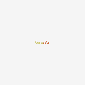
 The number of electrons in each of arsenic's shells is 2, 8, 18, 5 and its electron configuration is [Ar] 3d10 4s2 4p3. The arsenic atom has a radius of 119 pm and a Van der Waals radius of 185 pm. Arsenic was discovered in the early Bronze Age, circa 2500 BC. It was first isolated by Albertus Magnus in 1250 AD. In its elemental form, arsenic is a metallic grey, brittle, crystalline, semimetallic solid.
  Arsenic is found in numerous minerals including arsenolite (As2O3), arsenopyrite (FeAsS), loellingite (FeAs2), orpiment (As2S3), and realgar (As4S4). Arsenic has numerous applications as a semiconductor and other electronic applications as indium arsenide, silicon arsenide and tin arsenide. Arsenic is finding increasing uses as a doping agent in solid-state devices such as transistors.
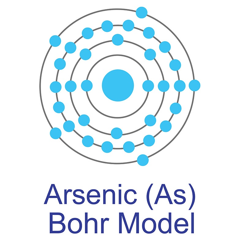
 Gallium was predicted by Dmitri Mendeleev in 1871. It was first discovered and isolated by Lecoq de Boisbaudran in 1875. In its elemental form, gallium has a silvery appearance.
  Gallium is one of three elements that occur naturally as a liquid at room temperature, the other two being