SECTION 1. IDENTIFICATION
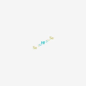
Product Name: Hafnium Selenide
Product Number: All applicable American Elements product codes, e.g. HF-SE-02
, HF-SE-03
, HF-SE-04
, HF-SE-05
CAS #: 12162-21-9
Relevant identified uses of the substance: Scientific research and development
Supplier details:
American Elements
10884 Weyburn Ave.
Los Angeles, CA 90024
Tel: +1 310-208-0551
Fax: +1 310-208-0351
Emergency telephone number:
Domestic, North America: +1 800-424-9300
International: +1 703-527-3887
SECTION 2. HAZARDS IDENTIFICATION
Classification of the substance or mixture in accordance with 29 CFR 1910 (OSHA HCS)
GHS06 Skull and crossbones
Acute Tox. 3 H301 Toxic if swallowed.
Acute Tox. 3 H331 Toxic if inhaled.
GHS08 Health hazard
STOT RE 2 H373 May cause damage to the central nervous system, the kidneys, the liver, the reproductive system, the digestive system and the blood through prolonged or repeated exposure. Route of exposure: Oral, Inhalative.
Hazards not otherwise classified
No data available
GHS label elements
GHS label elements, including precautionary statements
Hazard pictograms


GHS06 GHS08
Signal word
Danger
Hazard statements
H301+H331 Toxic if swallowed or if inhaled.
H373
May cause damage to the central nervous system, the kidneys, the liver, the reproductive system, the digestive system and the blood through prolonged or repeated exposure. Route of exposure: Oral, Inhalative.
Precautionary statements
P260
Do not breathe dust/fume/gas/mist/vapors/spray.
P261
Avoid breathing dust/fume/gas/mist/vapors/spray.
P301+P310 IF SWALLOWED: Immediately call a POISON CENTER/ doctor/...
P304+P340 IF INHALED: Remove person to fresh air and keep comfortable for breathing.
P405
Store locked up.
P501
Dispose of contents/container in accordance with local/regional/national/international regulations.
WHMIS classification
D1A - Very toxic material causing
immediate and serious toxic effects
D2A - Very toxic material causing other toxic effects
Classification system
HMIS ratings (scale 0-4)
(Hazardous Materials Identification System)
Health (acute effects) = 2
Flammability = 0
Physical Hazard = 1
Other hazards
Results of PBT and vPvB assessment
PBT:
N/A
vPvB:
N/A
SECTION 3. COMPOSITION/INFORMATION ON INGREDIENTS
Substances
CAS No. / Substance Name:
12162-21-9 - Hafnium Selenide
SECTION 4. FIRST AID MEASURES
Description of first aid measures
General information
Immediately remove any clothing soiled by the product.
Remove breathing apparatus only after contaminated clothing has been completely removed.
In case of irregular breathing or respiratory arrest provide artificial respiration.
If inhaled:
Supply patient with fresh air. If not breathing, provide artificial respiration. Keep patient warm.
Seek immediate medical advice.
In case of skin contact:
Immediately wash with soap and water; rinse thoroughly.
Seek immediate medical advice.
In case of eye contact:
Rinse opened eye for several minutes under running water. Consult a physician.
If swallowed:
Do not induce vomiting; immediately call for medical help.
Information for doctor
Most important symptoms and effects, both acute and delayed
No data available
Indication of any immediate medical attention and special treatment needed
No data available
SECTION 5. FIREFIGHTING MEASURES
Extinguishing media
Suitable extinguishing agents
Product is not flammable. Use fire-fighting measures that suit the surrounding fire.
Special hazards arising from the substance or mixture
If this product is involved in a fire, the following can be released:
Toxic metal oxide fume
Hydrogen selenide
Advice for firefighters
Protective equipment:
Wear self-contained respirator.
Wear fully protective impervious suit.
SECTION 6. ACCIDENTAL RELEASE MEASURES
Personal precautions, protective equipment and emergency procedures
Use personal protective equipment. Keep unprotected persons away.
Ensure adequate ventilation
Environmental precautions:
Do not allow material to be released to the environment without official permits.
Methods and materials for containment and cleanup:
Dispose of contaminated material as waste according to section 13.
Ensure adequate ventilation.
Prevention of secondary hazards:
No special measures required.
Reference to other sections
See Section 7 for information on safe handling
See Section 8 for information on personal protection equipment.
See Section 13 for disposal information.
SECTION 7. HANDLING AND STORAGE
Handling
Precautions for safe handling
Keep container tightly sealed.
Store in cool, dry place in tightly closed containers.
Ensure good ventilation at the workplace.
Open and handle container with care.
Information about protection against explosions and fires:
The product is not flammable
Conditions for safe storage, including any incompatibilities
Requirements to be met by storerooms and receptacles:
No special requirements.
Information about storage in one common storage facility:
Do not store together with acids.
Store away from oxidizing agents.
Further information about storage conditions:
Keep container tightly sealed.
Store in cool, dry conditions in well-sealed containers.
Specific end use(s)
No data available
SECTION 8. EXPOSURE CONTROLS/PERSONAL PROTECTION
Additional information: No data
Exposure controls
Personal protective equipment
Follow typical protective and hygienic practices for handling chemicals.
Keep away from foodstuffs, beverages and feed.
Remove all soiled and contaminated clothing immediately.
Wash hands before breaks and at the end of work.
Store protective clothing separately.
Maintain an ergonomically appropriate working environment.
Breathing equipment:
Use self-contained respiratory protective device in emergency situations.
Protection of hands:
Impervious gloves
Inspect gloves prior to use.
Suitability of gloves should be determined both by material and quality, the latter of which may vary by manufacturer.
Penetration time of glove material (in minutes)
No data available
Eye protection: Safety glasses
Body protection: Protective work clothing.
SECTION 9. PHYSICAL AND CHEMICAL PROPERTIES
Information on basic physical and chemical properties
Appearance:
Form: Various forms (powder/flake/crystalline/beads, etc.)
Odor threshold: No data available.
pH: N/A
Melting point/Melting range: >1350 °C (>2462 °F)
Boiling point/Boiling range: No data available
Sublimation temperature / start: No data available
Flammability (solid, gas)
No data available.
Ignition temperature: No data available
Decomposition temperature: No data available
Autoignition: No data available.
Danger of explosion: No data available.
Explosion limits:
Lower: No data available
Upper: No data available
Vapor pressure: N/A
Density at 20 °C (68 °F): 5.81 g/cm3 (48.484 lbs/gal)
Relative density
No data available.
Vapor density
N/A
Evaporation rate
N/A
Solubility in Water (H2O): Insoluble
Partition coefficient (n-octanol/water): No data available.
Viscosity:
Dynamic: N/A
Kinematic: N/A
Other information
No data available
SECTION 10. STABILITY AND REACTIVITY
Reactivity
No data available
Chemical stability
Stable under recommended storage conditions.
Thermal decomposition / conditions to be avoided:
Decomposition will not occur if used and stored according to specifications.
Possibility of hazardous reactions
Reacts with strong oxidizing agents
Conditions to avoid
No data available
Incompatible materials:
Acids
Oxidizing agents
Hazardous decomposition products:
Toxic metal oxide fume
Hydrogen selenide
SECTION 11. TOXICOLOGICAL INFORMATION
Information on toxicological effects
Acute toxicity:
Toxic if inhaled.
Toxic if swallowed.
LD/LC50 values that are relevant for classification:
Oral LD50 >5000 mg/kg (rat)
Skin irritation or corrosion:
May cause irritation
Eye irritation or corrosion:
May cause irritation
Sensitization:
No sensitizing effects known.
Germ cell mutagenicity:
No effects known.
Carcinogenicity:
IARC-1: Carcinogenic to humans: sufficient evidence of carcinogenicity.
EPA-B1: Probable human carcinogen, limited evidence of carcinogenicity from epidemiologic studies.
Carcinogen as defined by OSHA.
ACGIH A2: Suspected human carcinogen: Agent is carcinogenic in experimental animals at dose levels, by route(s) of administration, at site(s), of histologic type(s), or by mechanism(s) considered relevant to worker exposure. Available epidemiologic studies are conflicting or insufficient to
confirm an increased risk of cancer in exposed humans.
NTP-K: Known to be carcinogenic: sufficient evidence from human studies.
Reproductive toxicity:
No effects known.
Specific target organ system toxicity - repeated exposure:
May cause damage to the central nervous system, the kidneys, the liver, the reproductive system, the digestive system and the blood through prolonged or repeated exposure. Route of exposure: Oral, Inhalative.
Specific target organ system toxicity - single exposure:
No effects known.
Aspiration hazard:
No effects known.
Subacute to chronic toxicity:
No effects known.
Additional toxicological information:
To the best of our knowledge the acute and chronic toxicity of this substance is not fully known.
SECTION 12. ECOLOGICAL INFORMATION
Toxicity
Aquatic toxicity:
No data available
Persistence and degradability
No data available
Bioaccumulative potential
No data available
Mobility in soil
No data available
Ecotoxical effects:
Remark:
Very toxic for aquatic organisms
Additional ecological information:
Do not allow material to be released to the environment without official permits.
Do not allow product to reach groundwater, water courses, or sewage systems, even in small quantities.
Danger to drinking water if even extremely small quantities leak into the ground.
Also poisonous for fish and plankton in water bodies.
May cause long lasting harmful effects to aquatic life.
Avoid transfer into the environment.
Very toxic for aquatic organisms
Results of PBT and vPvB assessment
PBT:
N/A
vPvB:
N/A
Other adverse effects
No data available
SECTION 13. DISPOSAL CONSIDERATIONS
Waste treatment methods
Recommendation
Consult official regulations to ensure proper disposal.
Uncleaned packagings:
Recommendation:
Disposal must be made according to official regulations.
SECTION 14. TRANSPORT INFORMATION
UN-Number
DOT, IMDG, IATA
UN3077
UN proper shipping name
DOT
Environmentally hazardous substances, solid, n.o.s. (Hafnium selenide)
IMDG, IATA
ENVIRONMENTALLY HAZARDOUS SUBSTANCE, SOLID, N.O.S. (Hafnium selenide)
Transport hazard class(es)
DOT, IMDG
Class: 9 Miscellaneous dangerous substances and articles.
Label: 9
Class: 9 (M7) Miscellaneous dangerous substances and articles
Label: 9
IATA
Class: 9 Miscellaneous dangerous substances and articles.
Label: 9
Packing group
DOT, IMDG, IATA: III
Environmental hazards:
Special marking (ADR):
Symbol (fish and tree)
Special marking (IATA):
Symbol (fish and tree)
Special precautions for user
Warning: Miscellaneous dangerous substances and articles
EMS Number: F-A,S-F
Transport in bulk according to Annex II of MARPOL73/78 and the IBC Code
N/A
Transport/Additional information:
DOT
Marine Pollutant (DOT): No
UN "Model Regulation": UN3077, Environmentally hazardous substances, solid, n.o.s. (Hafnium selenide), 9, III
SECTION 15. REGULATORY INFORMATION
Safety, health and environmental regulations/legislation specific for the substance or mixture
GHS GHS label elements, including precautionary statements
Hazard pictograms
GHS06
GHS08
Signal word
Danger
Hazard statements
H301+H331 Toxic if swallowed or if inhaled.
H373
May cause damage to the central nervous system, the kidneys, the liver, the reproductive system, the digestive system and the blood through prolonged or repeated exposure. Route of exposure: Oral, Inhalative.
Precautionary statements
P260
Do not breathe dust/fume/gas/mist/vapors/spray.
P261
Avoid breathing dust/fume/gas/mist/vapors/spray.
P301+P310 IF SWALLOWED: Immediately call a POISON CENTER/ doctor/...
P304+P340 IF INHALED: Remove person to fresh air and keep comfortable for breathing.
P405
Store locked up.
P501
Dispose of contents/container in accordance with local/regional/national/international regulations.
National regulations
All components of this product are listed in the U.S. Environmental Protection Agency Toxic Substances Control Act Chemical substance Inventory.
All components of this product are listed on the Canadian Domestic Substances List (DSL).
SARA Section 313 (specific toxic chemical listings)
1306-24-7 Cadmium selenide
California Proposition 65
Prop 65 - Chemicals known to cause cancer
1306-24-7 Cadmium selenide
Prop 65 - Developmental toxicity
Substance is not listed.
Prop 65 - Developmental toxicity, female
Substance is not listed.
Prop 65 - Developmental toxicity, male
Substance is not listed.
Information about limitation of use:
For use only by technically qualified individuals.
This product is subject to the reporting requirements of section 313 of the Emergency Planning and Community Right to Know Act of 1986 and 40CFR372.
Other regulations, limitations and prohibitive regulations
Substance of Very High Concern (SVHC) according to the REACH Regulations (EC) No. 1907/2006.
Substance is not listed.
The conditions of restrictions according to Article 67 and Annex XVII of the Regulation (EC) No 1907/2006 (REACH) for the manufacturing, placing on the market and use must be observed.
Substance is not listed.
Annex XIV of the REACH Regulations (requiring Authorisation for use)
Substance is not listed.
Chemical safety assessment:
A Chemical Safety Assessment has not been carried out.
SECTION 16. OTHER INFORMATION
Safety Data Sheet according to Regulation (EC) No. 1907/2006 (REACH). The above information is believed to be correct but does not purport to be all inclusive and shall be used only as a guide. The information in this document is based on the present state of our knowledge and is applicable to the product with regard to appropriate safety precautions. It does not represent any guarantee of the properties of the product. American Elements shall not be held liable for any damage resulting from handling or from contact with the above product. See reverse side of invoice or packing slip for additional terms and conditions of sale. COPYRIGHT 1997-2022 AMERICAN ELEMENTS. LICENSED GRANTED TO MAKE UNLIMITED PAPER COPIES FOR INTERNAL USE ONLY.
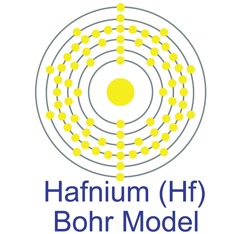 The number of electrons in each of Hafnium's shells is 2, 8, 18, 32, 10, 2 and its electron configuration is [Xe] 4f14 5d2 6s2. The hafnium atom has a radius of 159 pm and a Van der Waals radius of 212 pm. Hafnium was predicted by Dmitri Mendeleev in 1869 but it was not until 1922 that it was first isolated Dirk Coster and George de Hevesy. In its elemental form, hafnium has a lustrous silvery-gray appearance.
  Hafnium does not exist as a free element in nature. It is found in
 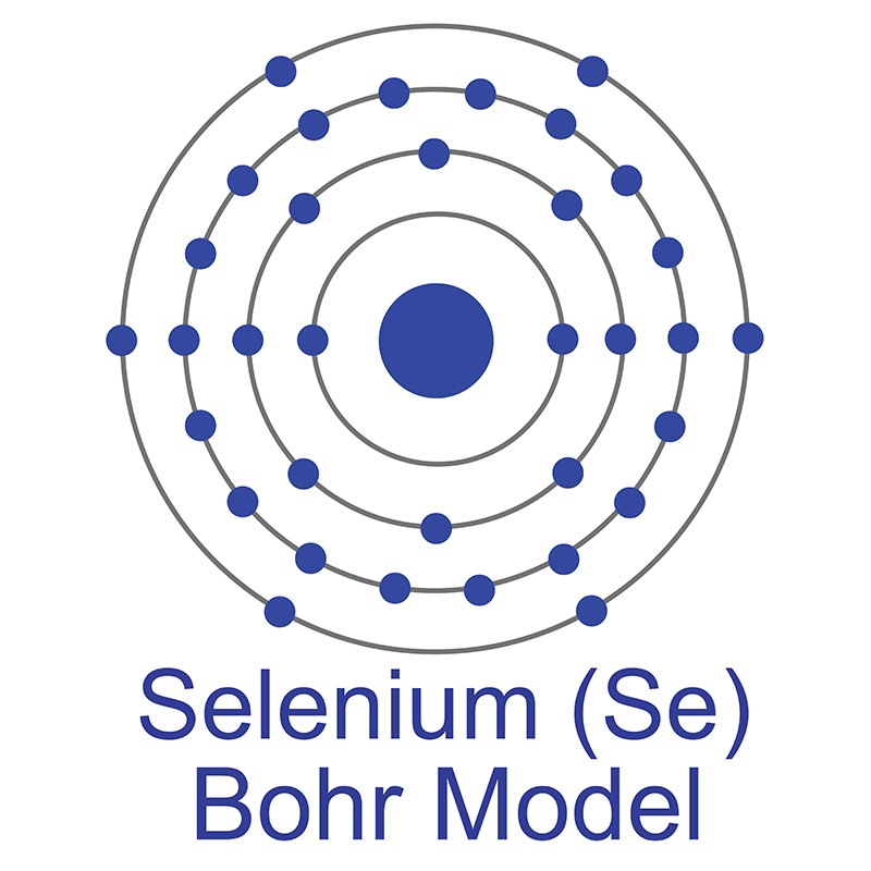 See more Selenium products.
 One of the most common uses for selenium is in