SECTION 1. IDENTIFICATION
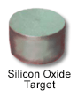
Product Name: Silicon Oxide Sputtering Target
Product Number: All applicable American Elements product codes, e.g. SI-OX-03-ST
, SI-OX-04-ST
, SI-OX-05-ST
CAS #: 7631-86-9
Relevant identified uses of the substance: Scientific research and development
Supplier details:
American Elements
10884 Weyburn Ave.
Los Angeles, CA 90024
Tel: +1 310-208-0551
Fax: +1 310-208-0351
Emergency telephone number:
Domestic, North America: +1 800-424-9300
International: +1 703-527-3887
SECTION 2. HAZARDS IDENTIFICATION
Classification of the substance or mixture
GHS Classification in accordance with 29 CFR 1910 (OSHA HCS)
Specific target organ toxicity - repeated exposure (Category 1), H372
Signal word: Danger
Hazard statement(s)
H372
Causes damage to organs through prolonged or repeated exposure.
Precautionary statement(s)
P260
Do not breathe dust/ fume/ gas/ mist/ Vapors/ spray.
P264
Wash skin thoroughly after handling.
P270
Do not eat, drink or smoke when using this product.
P314
Get medical advice/ attention if you feel unwell.
P501
Dispose of contents/ container to an approved waste disposal plant
SECTION 3. COMPOSITION/INFORMATION ON INGREDIENTS
Substances
Synonyms: Silicon dioxide
Formula: O2Si
Molecular Weight: 60.08 g/mol
CAS-No.: 7631-86-9
EC-No.: 231-545-4
Hazardous components
Component: Silicon dioxide
Classification: STOT RE1; H372
Concentration: 90-100%
SECTION 4. FIRST AID MEASURES
Description of first aid measures
General advice
Consult a physician. Show this safety data sheet to the doctor in attendance.
Move out of dangerous area.
If inhaled
If breathed in, move person into fresh air. If not breathing, give artificial respiration. Consult a physician.
In case of skin contact
Wash off with soap and plenty of water. Consult a physician.
In case of eye contact
Flush eyes with water as a precaution.
If swallowed
Never give anything by mouth to an unconscious person. Rinse mouth with water. Consult a physician.
Most important symptoms and effects, both acute and delayed
The most important known symptoms and effects are described in the labelling (see section 2.2) and/or in section 11
Indication of any immediate medical attention and special treatment needed: no data available
SECTION 5. FIREFIGHTING MEASURES
Extinguishing media
Suitable extinguishing media
Use water spray, alcohol-resistant foam, dry chemical or carbon dioxide.
Special hazards arising from the substance or mixture
silicon oxides
Advice for firefighters
Wear self contained breathing apparatus for fire fighting if necessary.
Further information
no data available
SECTION 6. ACCIDENTAL RELEASE MEASURES
Personal precautions, protective equipment and emergency procedures
Use personal protective equipment. Avoid dust formation. Avoid breathing Vapors, mist or gas. Avoid breathing dust.
For personal protection see section 8.
Environmental precautions
Do not let product enter drains.
Methods and materials for containment and cleaning up
Pick up and arrange disposal without creating dust. Sweep up and shovel. Keep in suitable, closed containers for disposal.
Reference to other sections
For disposal see section 13.
SECTION 7. HANDLING AND STORAGE
Precautions for safe handling
Avoid formation of dust and aerosols.
Provide appropriate exhaust ventilation at places where dust is formed.
For precautions see section 2.2.
Conditions for safe storage, including any incompatibilities
Keep container tightly closed in a dry and well-ventilated place.
Specific end use(s)
Apart from the uses mentioned in section 1.2 no other specific uses are stipulated
SECTION 8. EXPOSURE CONTROLS/PERSONAL PROTECTION
Exposure controls
Appropriate engineering controls
Handle in accordance with good industrial hygiene and safety practice. Wash hands before breaks and at the end of workday.
Personal protective equipment
Eye/face protection
Use equipment for eye protection tested and approved under appropriate government standards such as NIOSH (US) or EN 166(EU).
Skin protection
Handle with gloves. Gloves must be inspected prior to use. Use proper glove removal technique (without touching glove's outer surface) to avoid skin contact with this product. Dispose of contaminated gloves after use in accordance with applicable laws and good laboratory practices. Wash and dry hands.
Body Protection
Choose body protection in relation to its type, to the concentration and amount of dangerous substances, and to the specific work-place., The type of protective equipment must be selected according to the concentration and amount of the dangerous substance at the specific workplace.
Respiratory protection
Respiratory protection is not required. Where protection from nuisance levels of dusts are desired, use type N95 (US) or type P1 (EN 143) dust masks. Use respirators and components tested and approved under appropriate government standards such as NIOSH (US) or CEN (EU).
Control of environmental exposure
Do not let product enter drains.
SECTION 9. PHYSICAL AND CHEMICAL PROPERTIES
Information on basic physical and chemical properties
Appearance
Form: solid
Odor: no data available
Odor Threshold: no data available
pH: no data available
Melting point/freezing point
Melting point/range: > 1,600 °C (> 2,912 °F)
Initial boiling point and boiling range: 2,230 °C (4,046 °F)
Flash point: no data available
EVaporation rate: no data available
Flammability (solid, gas): no data available
Upper/lower flammability or explosive limits: no data available
Vapor pressure: no data available
Vapor density: no data available
Relative density: 2.600 g/cm3
Water solubility: insoluble
Partition coefficient: n-octanol/water: no data available
Auto-ignition temperature: no data available
Decomposition temperature: no data available
Viscosity: no data available
Explosive properties: no data available
Oxidizing properties: no data available
Other safety information: no data available
SECTION 10. STABILITY AND REACTIVITY
Reactivity: no data available
Chemical stability
Stable under recommended storage conditions.
Possibility of hazardous reactions: no data available
Conditions to avoid: no data available
Incompatible materials
Strong oxidizing agents
Hazardous decomposition products
In the event of fire: see section 5
SECTION 11. TOXICOLOGICAL INFORMATION
Information on toxicological effects
Acute toxicity
LD50 Oral - rat - 3,160 mg/kg
Inhalation: no data available
Dermal:
no data available
no data available
Skin corrosion/irritation: no data available
Serious eye damage/eye irritation: no data available
Respiratory or skin sensitisation: no data available
Germ cell mutagenicity
rat
Unscheduled DNA synthesis
Carcinogenicity
Carcinogenicity - rat - Inhalation
Tumorigenic:Carcinogenic by RTECS criteria. Lungs, Thorax, or Respiration:Tumors.
This product is or contains a component that is not classifiable as to its carcinogenicity based on its IARC, ACGIH, NTP, or EPA classification.
IARC: 3 - Group 3: Not classifiable as to its carcinogenicity to humans (Silicon dioxide)
ACGIH:
No component of this product present at levels greater than or equal to 0.1% is identified as a carcinogen or potential carcinogen by ACGIH.
NTP:
No component of this product present at levels greater than or equal to 0.1% is identified as a known or anticipated carcinogen by NTP.
OSHA:
No component of this product present at levels greater than or equal to 0.1% is identified as a carcinogen or potential carcinogen by OSHA.
Reproductive toxicity
no data available
no data available
Specific target organ toxicity - single exposure: no data available
Specific target organ toxicity - repeated exposure: no data available
The substance or mixture is classified as specific target organ toxicant, repeated exposure, category 1.
Aspiration hazard: no data available
Additional Information
RTECS: Not available
To the best of our knowledge, the chemical, physical, and toxicological properties have not been thoroughly investigated.
Stomach - Irregularities - Based on Human Evidence
Stomach - Irregularities - Based on Human Evidence
SECTION 12. ECOLOGICAL INFORMATION
Toxicity
no data available
Persistence and degradability: no data available
Bioaccumulative potential: no data available
Mobility in soil: no data available
Results of PBT and vPvB assessment
PBT/vPvB assessment not available as chemical safety assessment not required/not conducted
Other adverse effects: no data available
SECTION 13. DISPOSAL CONSIDERATIONS
Waste treatment methods
Product
Offer surplus and non-recyclable solutions to a licensed disposal company.
Contaminated packaging
Dispose of as unused product.
SECTION 14. TRANSPORT INFORMATION
DOT (US)
Not dangerous goods
IMDG
Not dangerous goods
IATA
Not dangerous goods
SECTION 15. REGULATORY INFORMATION
SARA 302
Components
SARA 302: No chemicals in this material are subject to the reporting requirements of SARA Title III, Section 302.
SARA 313
Components
SARA 313: This material does not contain any chemical components with known CAS numbers that exceed the threshold (De Minimis) reporting levels established by SARA Title III, Section 313.
SARA 311/312
Hazards
Chronic Health Hazard
Massachusetts Right To Know
Components
Silicon dioxide
CAS-No.: 7631-86-9
Revision Date: 1993-04-24
Pennsylvania Right To Know Components
Silicon dioxide
CAS-No.:7631-86-9
Revision Date: 1993-04-24
New Jersey Right To Know Components
Silicon dioxide
CAS-No.: 7631-86-9
Revision Date: 1993-04-24
California Prop. 65
Components
This product does not contain any chemicals known to State of California to cause cancer, birth defects, or any other reproductive harm
SECTION 16. OTHER INFORMATION
Safety Data Sheet according to Regulation (EC) No. 1907/2006 (REACH). The above information is believed to be correct but does not purport to be all inclusive and shall be used only as a guide. The information in this document is based on the present state of our knowledge and is applicable to the product with regard to appropriate safety precautions. It does not represent any guarantee of the properties of the product. American Elements shall not be held liable for any damage resulting from handling or from contact with the above product. See reverse side of invoice or packing slip for additional terms and conditions of sale. COPYRIGHT 1997-2022 AMERICAN ELEMENTS. LICENSED GRANTED TO MAKE UNLIMITED PAPER COPIES FOR INTERNAL USE ONLY.
 The number of electrons in each of Silicon's shells is 2, 8, 4 and its electron configuration is [Ne] 3s2 3p2. The silicon atom has a radius of 111 pm and a Van der Waals radius of 210 pm. Silicon was discovered and first isolated by Jöns Jacob Berzelius in 1823. Silicon makes up 25.7% of the earth's crust, by weight, and is the second most abundant element, exceeded only by oxygen. The metalloid is rarely found in pure crystal form and is usually produced from the iron-silicon alloy ferrosilicon.
  Silica (or