SECTION 1. IDENTIFICATION
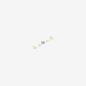
Product Name: Tungsten Telluride
Product Number: All applicable American Elements product codes, e.g. W-TE-05-I
, W-TE-05-L
, W-TE-05-P
, W-TE-05-ST
, W-TE-05-WF
CAS #: 12067-76-4
Relevant identified uses of the substance: Scientific research and development
Supplier details:
American Elements
10884 Weyburn Ave.
Los Angeles, CA 90024
Tel: +1 310-208-0551
Fax: +1 310-208-0351
Emergency telephone number:
Domestic, North America: +1 800-424-9300
International: +1 703-527-3887
SECTION 2. HAZARDS IDENTIFICATION
Routes of entry: Inhalation? Yes Skin? Yes Eyes? Yes Ingestion? Yes
Signs and Symptoms of Overexposure:
Inhalation: May cause a red, dry throat, coughing, dry mouth, garlic-like odor to breath, sweat and urine, loss of appetite, sleepiness and nausea.
Ingestion: May cause a dry mouth, garlic-like odor to breath, sweat and urine, loss of appetite, sleepiness and nausea.
Skin: May cause redness and itching.
Eye: May cause redness and itching.
Health Hazards (Acute and Chronic):
Inhalation:
Acute: May cause irritation to the respiratory system, a dry mouth, garlic odor to breath, sweat and urine.
Chronic: May cause anorexia, nausea, depression, somnolence and pulmonary fibrosis.
Ingestion:
Acute: May cause a dry mouth, suppression of sweat, garlic odor to breath and urine.
Chronic: May cause anorexia, nausea, depression, somnolence.
Skin:
Acute: May cause irritation and itching.
Chronic: May cause dermatitis.
Eye:
Acute: May cause irritation.
Chronic: No chronic health effects recorded.
Target Organs: May affect the skin and central nervous system.
Carcinogenicity: NTP? No IARC Monographs? No OSHA Regulated? No
Medical Conditions Aggravated by Exposure: Pre-existing skin disorders.
Hazard symbols:

T Toxic
Risk phrases:
Toxic if swallowed.
Irritating to eyes, respiratory system and skin.
Safety phrases:
When using do not eat or drink.
In case of contact with eyes, rinse immediately with plenty of water and seek medical advice.
Wear suitable protective clothing and gloves.
In case of accident or if you feel unwell, seek medical advice immediately.
This material and its container must be disposed of as hazardous waste.
SECTION 3. COMPOSITION/INFORMATION ON INGREDIENTS
Molecular weight: 439.05
SECTION 4. FIRST AID MEASURES
Inhalation: Remove victim to fresh air, keep warm and quiet, and give oxygen if breathing is difficult; seek medical attention.
Ingestion: Give 1-2 glasses of milk or water and induce vomiting, seek medical attention. Never induce vomiting or give anything by mouth to an unconscious person.
Skin: Remove contaminated clothing, brush material off skin, wash affected area with mild soap and water, and seek medical attention if symptoms persist.
Eye: Flush eyes with lukewarm water, lifting upper and lower eyelids for at least 15 minutes and seek medical attention. Seek medical attention if symptoms persist.
SECTION 5. FIREFIGHTING MEASURES
Method Used: Unknown Explosive Limits: LEL: N/A UEL: N/A
Extinguishing Media: Use suitable extinguishing agent for surrounding material and type of fire
Special Fire Fighting Procedures:
Firefighters must wear full face, self-contained breathing apparatus with full protective clothing to prevent contact with skin and eyes. Fumes from fire are hazardous. Isolate runoff to prevent
environmental pollution.
Unusual Fire and Explosion Hazards:
When heated to decomposition, tungsten telluride may emit toxic fumes of tellurium.
SECTION 6. ACCIDENTAL RELEASE MEASURES
Steps to be taken in case material is released or spilled:
Wear appropriate respiratory and protective equipment specified in section VIII. Isolate spill area, provide ventilation and extinguish sources of ignition. Vacuum up spill using a high efficiency particulate absolute (HEPA) air filter and place in a closed container for proper disposal. Takecare not to raise dust.
Waste disposal method:
Dispose of in accordance with state, local, and federal regulations.
Hazard Label Information:
Store in cool, dry area and in tightly sealed container. Wash thoroughly after handling.
SECTION 7. HANDLING AND STORAGE
Precautions:
Do not breathe dust. Wear suitable protective clothing In case of insufficient ventilation, wear suitable respiratory equipment If you feel unwell, seek medical attention and show the label when possible. Avoid contact with skin and eyes
Storage:
No specific storage is required. Use shelves or cabinets sturdy enough to bear the weight of the chemicals. Be sure that it is not necessary to strain to reach materials, and that shelves are not overloaded.
SECTION 8. EXPOSURE CONTROLS/PERSONAL PROTECTION
Protective Equipment Summary (Hazard Label Information):
NIOSH approved respirator, impervious gloves, safety glasses, clothes to prevent contact.
Ventilation:
Local Exhaust: To maintain concentration at low exposure levels.
Mechanical (General): Recommended.
Work/Hygienic/Maintenance Practices:
Implement engineering and work practice controls to reduce and maintain concentration of exposure at low levels. Use good housekeeping and sanitation practices. Do not use tobacco or food in work area. Wash thoroughly before eating or smoking. Do not blow dust off clothing or skin with compressed air.
SECTION 9. PHYSICAL AND CHEMICAL PROPERTIES
Physical States: Solid
Boiling Point: N/A Vapor Pressure (vs. air or mmHg): N/A
Melting Point: N/A Density: g/cm3 N/A
Evaporation Rate: N/A Flash Point: N/A
Solubility in water: Insoluble
Appearance and odor: Black crystalline pieces, no odor.
SECTION 10. STABILITY AND REACTIVITY
Stability: Stable
Conditions to Avoid (instability): None
Incompatibility (materials to be avoided): None recorded
Hazardous Decomposition or Byproducts: Fumes of tellurium.
Hazardous Polymerization: Will not occur
Conditions to avoid (hazardous polymerization): None
SECTION 11. TOXICOLOGICAL INFORMATION
See Section 2
SECTION 12. ECOLOGICAL INFORMATION
Elimination information (persistence and degradability)
no data available
Ecotoxicity effects
no data available
Further information on ecology
no data available
SECTION 13. DISPOSAL CONSIDERATIONS
Product
Observe all federal, state, and local environmental regulations.
Contaminated packaging
Dispose of as unused product.
SECTION 14. EXPOSURE CONTROLS/PERSONAL PROTECTION
DOT regulations:
Hazard class: 6.1
Identification number: UN3288
Packing group: III
Proper shipping name (technical
name): TOXIC SOLID, INORGANIC, N.O.S. (Tungsten telluride)
Label 6.1
Land transport ADR/RID (cross-border)
ADR/RID class: 6.1 (T5) Toxic substances
Danger code (Kemler): 60
UN-Number: 3288
Packaging group: III
Description of goods: 3288 TOXIC SOLID, INORGANIC, N.O.S.
(Tungsten telluride)
Maritime transport IMDG:
IMDG Class: 6.1
UN Number: 3288
Label 6.1
Packaging group: III
Proper shipping name: TOXIC SOLID, INORGANIC, N.O.S. (Tungsten telluride)
Air transport ICAO-TI and IATA-DGR:
ICAO/IATA Class: 6.1
UN/ID Number: 3288
Label 6.1
Packaging group: III
Proper shipping name: TOXIC SOLID, INORGANIC, N.O.S. (Tungsten telluride)
SECTION 15. REGULATORY INFORMATION
Hazard symbols:
T Toxic
Risk phrases:
25 Toxic if swallowed.
36/37/38 Irritating to eyes, respiratory system and skin.
Safety phrases:
20 When using do not eat or drink.
26 In case of contact with eyes, rinse immediately with plenty of water and seek medical advice.
36/37 Wear suitable protective clothing and gloves.
45 In case of accident or if you feel unwell, seek medical advice immediately.
60 This material and its container must be disposed of as hazardous waste.
National regulations
All components of this product are listed in the U.S. Environmental
Protection Agency Toxic Substances Control Act Chemical substance Inventory.
All components of this product are listed on the Canadian Domestic
Substances List (DSL).
Information about limitation of use:
For use only by technically qualified individuals.
SECTION 16. OTHER INFORMATION
Safety Data Sheet according to Regulation (EC) No. 1907/2006 (REACH). The above information is believed to be correct but does not purport to be all inclusive and shall be used only as a guide. The information in this document is based on the present state of our knowledge and is applicable to the product with regard to appropriate safety precautions. It does not represent any guarantee of the properties of the product. American Elements shall not be held liable for any damage resulting from handling or from contact with the above product. See reverse side of invoice or packing slip for additional terms and conditions of sale. COPYRIGHT 1997-2022 AMERICAN ELEMENTS. LICENSED GRANTED TO MAKE UNLIMITED PAPER COPIES FOR INTERNAL USE ONLY.
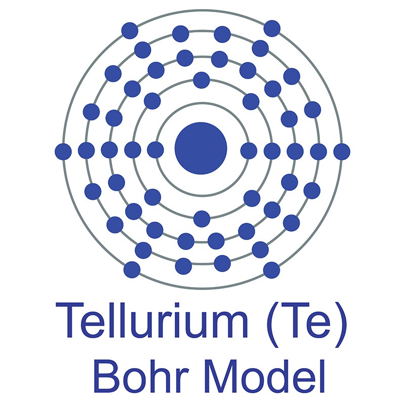 The number of electrons in each of tellurium's shells is 2, 8, 18, 18, 6 and its electron configuration is [Kr] 4d10 5s2 5p4. Tellurium was discovered by Franz Muller von Reichenstein in 1782 and first isolated by Martin Heinrich Klaproth in 1798. In its elemental form, tellurium has a silvery lustrous gray appearance. The tellurium atom has a radius of 140 pm and a Van der Waals radius of 206 pm.
  Tellurium is most commonly sourced from the anode sludges produced as a byproduct of copper refining. The name Tellurium originates from the Greek word Tellus, meaning Earth.
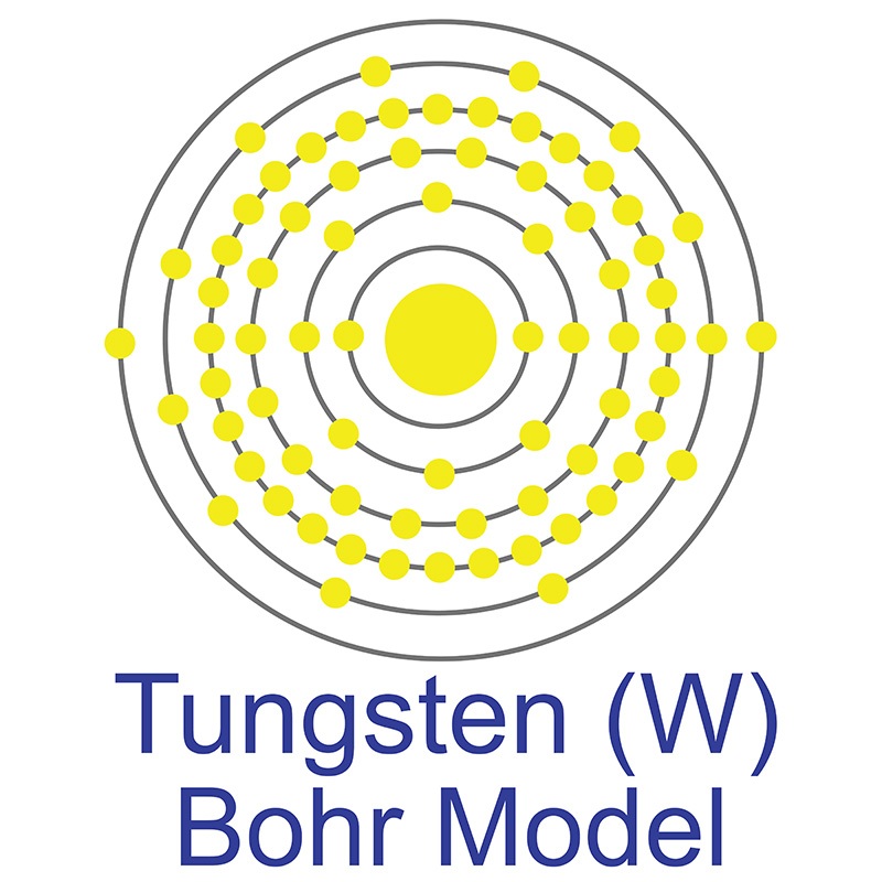 The tungsten atom has a radius of 139 pm and a Van der Waals radius of 210 pm. Tungsten was discovered by Torbern Bergman in 1781 and first isolated by Juan José Elhuyar and Fausto Elhuyar in 1783. In its elemental form, tungsten has a grayish white, lustrous appearance.
  Tungsten has the highest melting point of all the