See more Thorium products. Thorium (atomic symbol: Th, atomic number: 90) is a Block F, Group 3, Period 7 element with an atomic weight of 232.03806. The number of electrons in each of thorium's shells is [2, 8, 18, 32, 18, 10, 2] and its electron configuration is [Rn] 6d2 7s2. 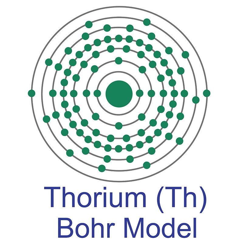 The thorium atom has a radius of 179 pm and a Van der Waals radius of 237 pm. Thorium was first discovered by Jöns Jakob Berzelius in 1829. The name Thorium originates from the Scandinavian god Thor, the Norse god of war and thunder.
  In its elemental form, thorium has a silvery, sometimes black-tarnished, appearance. It is found in small amounts in most rocks and soils. Thorium is a radioactive element that is currently the best contender for replacing uranium as nuclear fuel for nuclear reactors. It provides greater safety benefits, an absence of non-fertile isotopes, and it is both more available and abundant in the Earth's crust than uranium.
Materials
Materials by Form
2D Materials Alloy & Alloy Forms Pure Metals & Metal FormsCeramic FibersFoams: Metallic & Ceramic High Purity Materials Isotopes MXenesOxides Rare Earths Semiconductors Solutions
Chemicals & Salts
All Chemicals & Salts Acetates Aluminides Ammonium Sulfates Antimonides Arsenates Benzoate Bromates Bromides Carbonates Chlorides Chromates Fluorides Hydrides Hydroxides Iodates Iodides Lactates Molybdates Nitrates Oxalates Oxides Perchlorates Phosphates Selenates Selenides Selenites Silicates Stearates Sulfates Sulfides Sulfites Tantalates Tellurates Tellurides Tellurites ThiocyanatesVanadates
Ceramics
Nanomaterials
Organometallics
Materials by Application
Additive Manufacturing & 3D Printing Battery & Supercapacitor Materials Catalysts Dental Materials Electronics Materials Fuel Cell Materials Fusion EnergyGlass Manufacturing Green Technology & Alternative Energy Hydrogen Storage Laser Crystals Life Sciences & Biomaterials Metallurgy Nanotechnology & Nanomaterials Optical Materials Photovoltaic & Solar Energy Plating Pigments & Coatings Research & Development Space Technology Sputtering Targets Thin Film Deposition Water Treatment Weather Modification
Life Science Chemicals
Life Science Products AlcoholsAldehydesAmidesAminesAmino Acids & DerivativesAromaticsArylsAzetidinesBenzimidazolesBenzisoxazolesBenzodioxansBenzofuransBenzothiazolesBenzothiophenesBenzoxazolesCarboxylic AcidsEnzymes & InhibitorsEstersEthersFluorinated Building BlocksFuransHalidesImidazolesImidazolidinesIndazolesIndolesIndolinesIsoquinolinesIsoxazolesKetonesMorpholinesNaphthyridinesNitrilesOrganoboronOrganosiliconOxadiazolesOxazolesPharmaceuticals & IntermediatesPhenolsPhytochemicalsPiperazinesPiperidinesPyrazinesPyrazolesPyridazinesPyridinesPyrimidinesPyrrolesPyrrolidinesPyrrolinesQuinazolinesQuinolinesQuinoxalinesSpiroesSulfonyl ChloridesTetrahydroisoquinolinesTetrahydropyransTetrahydroquinolinesTetrazolesThiadiazolesThiazolesThiazolidinesThiolsThiophenesTriazinesTriazoles
About Us
Locations
Austria Belgium Brazil Canada China & Hong Kong Czech Republic Denmark Finland France Germany Greece Hungary India Indonesia Israel Italy Japan Malaysia Mexico Netherlands Norway Philippines Poland Portugal Russia Singapore South Korea Spain Sweden Switzerland Taiwan Thailand Turkey United Kingdom United States
Industries
Aerospace Agriculture Automotive Chemical Manufacturing Defense Dentistry Electronics Energy Storage & Batteries Fine Art Materials Fuel CellsFusion Energy Glass Investment Grade Metals Jewelry & Fashion Lasers Lighting Medical Devices Museums & Galleries Nuclear Energy Oil & Gas Optics Paper & Pulp Pharmaceuticals & Cosmetics Research & Laboratory Robotics Solar Energy Space Sports Equipment Steel & Alloy Producers Textiles & Fabrics Water Treatment Municipalities
Follow Us