See more Hafnium products. Hafnium (atomic symbol: Hf, atomic number: 72) is a Block D, Group 4, Period 6 element with an atomic weight of 178.49. 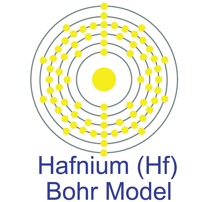 The number of electrons in each of Hafnium's shells is 2, 8, 18, 32, 10, 2 and its electron configuration is [Xe] 4f14 5d2 6s2. The hafnium atom has a radius of 159 pm and a Van der Waals radius of 212 pm. Hafnium was predicted by Dmitri Mendeleev in 1869 but it was not until 1922 that it was first isolated Dirk Coster and George de Hevesy. In its elemental form, hafnium has a lustrous silvery-gray appearance.
  Hafnium does not exist as a free element in nature. It is found in zirconium compounds such as zircon. Hafnium is often a component of superalloys and circuits used in semiconductor device fabrication. Its name is derived from the Latin word Hafnia, meaning Copenhagen, where it was discovered.
Materials
Materials by Form
2D Materials Alloy & Alloy Forms Pure Metals & Metal FormsCeramic FibersFoams: Metallic & Ceramic High Purity Materials Isotopes MXenesOxides Rare Earths Semiconductors Solutions
Chemicals & Salts
All Chemicals & Salts Acetates Aluminides Ammonium Sulfates Antimonides Arsenates Benzoate Bromates Bromides Carbonates Chlorides Chromates Fluorides Hydrides Hydroxides Iodates Iodides Lactates Molybdates Nitrates Oxalates Oxides Perchlorates Phosphates Selenates Selenides Selenites Silicates Stearates Sulfates Sulfides Sulfites Tantalates Tellurates Tellurides Tellurites ThiocyanatesVanadates
Ceramics
Nanomaterials
Organometallics
Materials by Application
Additive Manufacturing & 3D Printing Battery & Supercapacitor Materials Catalysts Dental Materials Electronics Materials Fuel Cell Materials Fusion EnergyGlass Manufacturing Green Technology & Alternative Energy Hydrogen Storage Laser Crystals Life Sciences & Biomaterials Metallurgy Nanotechnology & Nanomaterials Optical Materials Photovoltaic & Solar Energy Plating Pigments & Coatings Research & Development Space Technology Sputtering Targets Thin Film Deposition Water Treatment Weather Modification
Life Science Chemicals
Life Science Products AlcoholsAldehydesAmidesAminesAmino Acids & DerivativesAromaticsArylsAzetidinesBenzimidazolesBenzisoxazolesBenzodioxansBenzofuransBenzothiazolesBenzothiophenesBenzoxazolesCarboxylic AcidsEnzymes & InhibitorsEstersEthersFluorinated Building BlocksFuransHalidesImidazolesImidazolidinesIndazolesIndolesIndolinesIsoquinolinesIsoxazolesKetonesMorpholinesNaphthyridinesNitrilesOrganoboronOrganosiliconOxadiazolesOxazolesPharmaceuticals & IntermediatesPhenolsPhytochemicalsPiperazinesPiperidinesPyrazinesPyrazolesPyridazinesPyridinesPyrimidinesPyrrolesPyrrolidinesPyrrolinesQuinazolinesQuinolinesQuinoxalinesSpiroesSulfonyl ChloridesTetrahydroisoquinolinesTetrahydropyransTetrahydroquinolinesTetrazolesThiadiazolesThiazolesThiazolidinesThiolsThiophenesTriazinesTriazoles
About Us
Locations
Austria Belgium Brazil Canada China & Hong Kong Czech Republic Denmark Finland France Germany Greece Hungary India Indonesia Israel Italy Japan Malaysia Mexico Netherlands Norway Philippines Poland Portugal Russia Singapore South Korea Spain Sweden Switzerland Taiwan Thailand Turkey United Kingdom United States
Industries
Aerospace Agriculture Automotive Chemical Manufacturing Defense Dentistry Electronics Energy Storage & Batteries Fine Art Materials Fuel CellsFusion Energy Glass Investment Grade Metals Jewelry & Fashion Lasers Lighting Medical Devices Museums & Galleries Nuclear Energy Oil & Gas Optics Paper & Pulp Pharmaceuticals & Cosmetics Research & Laboratory Robotics Solar Energy Space Sports Equipment Steel & Alloy Producers Textiles & Fabrics Water Treatment Municipalities
Follow Us
 The number of electrons in each of Silicon's shells is 2, 8, 4 and its electron configuration is [Ne] 3s2 3p2. The silicon atom has a radius of 111 pm and a Van der Waals radius of 210 pm. Silicon was discovered and first isolated by Jöns Jacob Berzelius in 1823. Silicon makes up 25.7% of the earth's crust, by weight, and is the second most abundant element, exceeded only by oxygen. The metalloid is rarely found in pure crystal form and is usually produced from the iron-silicon alloy ferrosilicon.
  Silica (or