SECTION 1. IDENTIFICATION
Product Name: Silicon Sulfide Sputtering Target
Product Number: All applicable American Elements product codes, e.g. SI-S-02
, SI-S-03
, SI-S-04
, SI-S-05
CAS #: 13759-10-9
Relevant identified uses of the substance: Scientific research and development
Supplier details:
American Elements
10884 Weyburn Ave.
Los Angeles, CA 90024
Tel: +1 310-208-0551
Fax: +1 310-208-0351
Emergency telephone number:
Domestic, North America: +1 800-424-9300
International: +1 703-527-3887
SECTION 2. HAZARDS IDENTIFICATION
Classification of the substance or mixture
Classification according to Regulation (EC) No 1272/2008
GHS02 Flame
Water-react. 2 H261 In contact with water releases flammable gas.
GHS06 Skull and crossbones
Acute Tox. 2 H300 Fatal if swallowed.
GHS07
Skin Irrit. 2 H315 Causes skin irritation.
Eye Irrit. 2A H319 Causes serious eye irritation.
STOT SE 3 H335 May cause respiratory irritation.
Classification according to Directive 67/548/EEC or Directive 1999/45/EC
T; Toxic
R25: Toxic if swallowed.
Xi; Irritant
R36/37/38: Irritating to eyes, respiratory system and skin.
R31: Contact with acids liberates toxic gas.
Information concerning particular hazards for human and environment:
N/A
Hazards not otherwise classified
No data available
Label elements
Labelling according to Regulation (EC) No 1272/2008
The substance is classified and labeled according to the CLP regulation.
Hazard pictograms


GHS02 GHS06
Signal word: Danger
Hazard statements
H261 In contact with water releases flammable gas.
H300 Fatal if swallowed.
H315 Causes skin irritation.
H319 Causes serious eye irritation.
H335 May cause respiratory irritation.
Precautionary statements
P231+P232 Handle under inert gas. Protect from moisture.
P261 Avoid breathing dust/fume/gas/mist/vapors/spray.
P301+P310 IF SWALLOWED: Immediately call a POISON CENTER/ doctor/...
P305+P351+P338 IF IN EYES: Rinse cautiously with water for several minutes. Remove contact lenses, if present and easy to do. Continue rinsing.
P405 Store locked up.
P501 Dispose of contents/container in accordance with local/regional/national/international regulations.
WHMIS classification
B6 - Reactive flammable material
D1A - Very toxic material causing immediate and serious toxic effects
D2B - Toxic material causing other toxic effects
Classification system
HMIS ratings (scale 0-4)
(Hazardous Materials Identification System)
HEALTH
FIRE
REACTIVITY
2
2
3
Health (acute effects) = 2
Flammability = 2
Physical Hazard = 3
Other hazards
Results of PBT and vPvB assessment
PBT: N/A
vPvB: N/A
SECTION 3. COMPOSITION/INFORMATION ON INGREDIENTS
Substances
CAS No. / Substance Name:
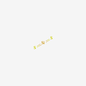
13759-10-9 Silicon (IV) sulfide
Identification number(s):
EC number: 237-344-8
SECTION 4. FIRST AID MEASURES
Description of first aid measures
General information
Immediately remove any clothing soiled by the product.
In case of irregular breathing or respiratory arrest provide artificial respiration.
If inhaled:
Supply patient with fresh air. If not breathing, provide artificial respiration. Keep patient warm.
Seek immediate medical advice.
In case of skin contact:
Immediately wash with soap and water; rinse thoroughly.
Seek immediate medical advice.
In case of eye contact:
Rinse opened eye for several minutes under running water. Consult a physician.
If swallowed:
Do not induce vomiting; immediately call for medical help.
Information for doctor
Most important symptoms and effects, both acute and delayed
No data available
Indication of any immediate medical attention and special treatment needed
No data available
SECTION 5. FIREFIGHTING MEASURES
Extinguishing media
Suitable extinguishing agents
CO2, sand, extinguishing powder. Do not use water.
Special hazards arising from the substance or mixture
If this product is involved in a fire, the following can be released:
Hydrogen sulfide
Sulfur oxides (SOx)
Silicon oxide
Advice for firefighters
Protective equipment:
Wear self-contained respirator.
Wear fully protective impervious suit.
SECTION 6. ACCIDENTAL RELEASE MEASURES
Personal precautions, protective equipment and emergency procedures
Mount respiratory protective device.
Use personal protective equipment. Keep unprotected persons away.
Ensure adequate ventilation
Environmental precautions:
Do not allow material to be released to the environment without official permits.
Do not allow product to enter drains, sewage systems, or other water courses.
Do not allow material to penetrate the ground or soil.
Methods and materials for containment and cleanup:
Dispose of contaminated material as waste according to section 13.
Ensure adequate ventilation.
Prevention of secondary hazards:
No special measures required.
Reference to other sections
See Section 7 for information on safe handling
See Section 8 for information on personal protection equipment.
See Section 13 for disposal information.
SECTION 7. HANDLING AND STORAGE
Handling
Precautions for safe handling
Keep container tightly sealed.
Store in cool, dry place in tightly closed containers.
Ensure good ventilation at the workplace.
Information about protection against explosions and fires:
Protect from humidity and water.
Reacts with acids forming hydrogen sulfide
Conditions for safe storage, including any incompatibilities
Requirements to be met by storerooms and receptacles:
No special requirements.
Information about storage in one common storage facility:
Store away from oxidizing agents.
Do not store together with acids.
Further information about storage conditions:
Keep container tightly sealed.
Store in cool, dry conditions in well-sealed containers.
Specific end use(s)
No data available
SECTION 8. EXPOSURE CONTROLS/PERSONAL PROTECTION
Additional information about design of technical systems:
Properly operating chemical fume hood designed for hazardous chemicals and having an average face velocity of at least 100 feet per minute.
Control parameters
Components with limit values that require monitoring at the workplace:
Not required.
Additional information: No data
Exposure controls
Personal protective equipment
Follow typical protective and hygienic practices for handling chemicals.
Keep away from foodstuffs, beverages and feed.
Remove all soiled and contaminated clothing immediately.
Wash hands before breaks and at the end of work.
Avoid contact with the eyes and skin.
Maintain an ergonomically appropriate working environment.
Breathing equipment:
Use suitable respirator when high concentrations are present.
Protection of hands:
Impervious gloves
Inspect gloves prior to use.
Suitability of gloves should be determined both by material and quality, the latter of which may vary by manufacturer.
Eye protection: Safety glasses
Body protection: Protective work clothing.
SECTION 9. PHYSICAL AND CHEMICAL PROPERTIES
Information on basic physical and chemical properties
Appearance:
Form: Powder
Color: White
Odor: Like rotten eggs
Odor threshold: No data available.
pH: N/A
Melting point/Melting range: 1090 °C (1994 °F)
Boiling point/Boiling range: No data available
Sublimation temperature / start: No data available
Flash point: N/A
Flammability (solid, gas): No data available.
Ignition temperature: No data available
Decomposition temperature: No data available
Autoignition: No data available.
Danger of explosion: Product does not present an explosion hazard.
Explosion limits:
Lower: No data available
Upper: No data available
Vapor pressure: N/A
Density at 20 °C (68 °F): 2.02 g/cm3 (16.857 lbs/gal)
Relative density: No data available.
Vapor density: N/A
Evaporation rate: N/A
Solubility in Water (H2O): No data available
Partition coefficient (n-octanol/water): No data available.
Viscosity:
Dynamic: N/A
Kinematic: N/A
Other information
No data available
SECTION 10. STABILITY AND REACTIVITY
Reactivity
Contact with acids liberates toxic gas.
Chemical stability
Stable under recommended storage conditions.
Thermal decomposition / conditions to be avoided:
Decomposition will not occur if used and stored according to specifications.
Possibility of hazardous reactions
Reacts with acids forming hydrogen sulfide
Contact with acids liberates toxic gas.
Conditions to avoid
No data available
Incompatible materials:
Oxidizing agents
Acids
Hazardous decomposition products:
Hydrogen sulfide
Sulfur oxides (SOx)
Silicon oxide
SECTION 11. TOXICOLOGICAL INFORMATION
Information on toxicological effects
Acute toxicity:
Fatal if swallowed.
LD/LC50 values that are relevant for classification: No data
Skin irritation or corrosion: Causes skin irritation.
Eye irritation or corrosion: Causes serious eye irritation.
Sensitization: No sensitizing effects known.
Germ cell mutagenicity: No effects known.
Carcinogenicity:
No classification data on carcinogenic properties of this material is available from the EPA, IARC, NTP, OSHA or ACGIH.
Reproductive toxicity: No effects known.
Specific target organ system toxicity - repeated exposure: No effects known.
Specific target organ system toxicity - single exposure: May cause respiratory irritation.
Aspiration hazard: No effects known.
Subacute to chronic toxicity:
Inorganic silicon compounds may be acute inhalation irritants. Prolonged inhalation may cause pulmonary fibrosis known as silicosis.
Subacute to chronic toxicity: No effects known.
Additional toxicological information:
To the best of our knowledge the acute and chronic toxicity of this substance is not fully known.
SECTION 12. ECOLOGICAL INFORMATION
Toxicity
Aquatic toxicity:
No data available
Persistence and degradability
No data available
Bioaccumulative potential
No data available
Mobility in soil
No data available
Additional ecological information:
Do not allow material to be released to the environment without official permits.
Do not allow undiluted product or large quantities to reach groundwater, water courses, or sewage systems.
Avoid transfer into the environment.
Results of PBT and vPvB assessment
PBT: N/A
vPvB: N/A
Other adverse effects
No data available
SECTION 13. DISPOSAL CONSIDERATIONS
Waste treatment methods
Recommendation
Consult official regulations to ensure proper disposal.
Uncleaned packagings:
Recommendation:
Disposal must be made according to official regulations
SECTION 14. TRANSPORT INFORMATION
UN-Number
DOT, IMDG, IATA
UN3134
UN proper shipping name
DOT
Water-reactive solid, toxic, n.o.s. (Silicon (IV) sulfide)
IMDG, IATA
WATER-REACTIVE SOLID, TOXIC, N.O.S. (Silicon (IV) sulfide)
Transport hazard class(es)
DOT
Class
4.3 Substances which, in contact with water, emit flammable gases.
Label
4.3+6.1
Class
4.3 (WT2) Substances which, in contact with water, emit flammable gases
Label
4.3+6.1
IMDG, IATA
Class
4.3 Substances which, in contact with water, emit flammable gases.
Label
4.3+6.1
Packing group
DOT, IMDG, IATA
II
Environmental hazards:
N/A
Special precautions for user
Warning: Substances which, in contact with water, emit flammable gases
Transport in bulk according to Annex II of MARPOL73/78 and the IBC Code
N/A
Transport/Additional information:
DOT
Marine Pollutant (DOT):
No
UN "Model Regulation":
UN3134, Water-reactive solid, toxic, n.o.s. (Silicon (IV) sulfide), 4.3 (6.1), II
SECTION 15. REGULATORY INFORMATION
Safety, health and environmental regulations/legislation specific for the substance or mixture
National regulations
All components of this product are listed in the U.S. Environmental Protection Agency Toxic Substances Control Act Chemical substance Inventory.
SARA Section 313 (specific toxic chemical listings)
Substance is not listed.
California Proposition 65
Prop 65 - Chemicals known to cause cancer
Substance is not listed.
Prop 65 - Developmental toxicity
Substance is not listed.
Prop 65 - Developmental toxicity, female
Substance is not listed.
Prop 65 - Developmental toxicity, male
Substance is not listed.
Information about limitation of use:
For use only by technically qualified individuals.
Other regulations, limitations and prohibitive regulations
Substance of Very High Concern (SVHC) according to the REACH Regulations (EC) No. 1907/2006.
Substance is not listed.
The conditions of restrictions according to Article 67 and Annex XVII of the Regulation (EC) No 1907/2006 (REACH) for the manufacturing, placing on the market and use must be observed.
Substance is not listed.
Annex XIV of the REACH Regulations (requiring Authorisation for use)
Substance is not listed.
REACH - Pre-registered substances
Substance is listed.
Chemical safety assessment:
A Chemical Safety Assessment has not been carried out.
SECTION 16. OTHER INFORMATION
Safety Data Sheet according to Regulation (EC) No. 1907/2006 (REACH). The above information is believed to be correct but does not purport to be all inclusive and shall be used only as a guide. The information in this document is based on the present state of our knowledge and is applicable to the product with regard to appropriate safety precautions. It does not represent any guarantee of the properties of the product. American Elements shall not be held liable for any damage resulting from handling or from contact with the above product. See reverse side of invoice or packing slip for additional terms and conditions of sale. COPYRIGHT 1997-2022 AMERICAN ELEMENTS. LICENSED GRANTED TO MAKE UNLIMITED PAPER COPIES FOR INTERNAL USE ONLY.
 The number of electrons in each of Silicon's shells is 2, 8, 4 and its electron configuration is [Ne] 3s2 3p2. The silicon atom has a radius of 111 pm and a Van der Waals radius of 210 pm. Silicon was discovered and first isolated by Jöns Jacob Berzelius in 1823. Silicon makes up 25.7% of the earth's crust, by weight, and is the second most abundant element, exceeded only by oxygen. The metalloid is rarely found in pure crystal form and is usually produced from the iron-silicon alloy ferrosilicon.
  Silica (or
 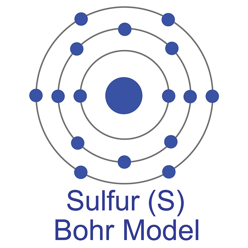 The number of electrons in each of Sulfur's shells is 2, 8, 6 and its electron configuration is [Ne] 3s2 3p4. In its elemental form, sulfur has a light yellow appearance. The sulfur atom has a covalent radius of 105 pm and a Van der Waals radius of 180 pm. In nature, sulfur can be found in hot springs, meteorites, volcanoes, and as galena, gypsum, and epsom salts. Sulfur has been known since ancient times but was not accepted as an element until 1777, when Antoine Lavoisier helped to convince the scientific community that it was an element and not a compound.