SECTION 1. IDENTIFICATION
Product Name: Silicon Chunk
Product Number: All applicable American Elements product codes, e.g. SI-E-02-CK
, SI-E-03-CK
, SI-E-04-CK
, SI-E-05-CK
, SI-E-06-CK
CAS #: 7440-21-3
Relevant identified uses of the substance: Scientific research and development
Supplier details:
American Elements
10884 Weyburn Ave.
Los Angeles, CA 90024
Tel: +1 310-208-0551
Fax: +1 310-208-0351
Emergency telephone number:
Domestic, North America: +1 800-424-9300
International: +1 703-527-3887
SECTION 2. HAZARDS IDENTIFICATION
Classification of the substance or mixture
Classification according to Regulation (EC) No 1272/2008
The substance is not classified as hazardous to health or the environment according to the CLP regulation.
Classification according to Directive 67/548/EEC or Directive 1999/45/EC
N/A
Information concerning particular hazards for human and environment:
No data available
Hazards not otherwise classified
No data available
Label elements
Labelling according to Regulation (EC) No 1272/2008
N/A
Hazard pictograms
N/A
Signal word
N/A
Hazard statements
N/A
WHMIS classification
Not controlled
Classification system
HMIS ratings (scale 0-4)
(Hazardous Materials Identification System)
HEALTH
FIRE
REACTIVITY
1
0
0
Health (acute effects) = 1
Flammability = 0
Physical Hazard = 0
Other hazards
Results of PBT and vPvB assessment
PBT:
N/A
vPvB:
N/A
SECTION 3. COMPOSITION/INFORMATION ON INGREDIENTS
Substances
CAS No. / Substance Name:
7440-21-3 Silicon
Identification number(s):
EC number:
231-130-8
SECTION 4. FIRST AID MEASURES
Description of first aid measures
General information
No special measures required.
If inhaled:
Seek medical treatment in case of complaints.
In case of skin contact:
Generally the product does not irritate the skin.
In case of eye contact:
Rinse opened eye for several minutes under running water. If symptoms persist, consult a doctor.
If swallowed:
If symptoms persist consult doctor.
Information for doctor
Most important symptoms and effects, both acute and delayed
No data available
Indication of any immediate medical attention and special treatment needed
No data available
SECTION 5. FIREFIGHTING MEASURES
Extinguishing media
Suitable extinguishing agents
Carbon dioxide, extinguishing powder or water spray. Fight larger fires with water spray or alcohol resistant foam.
Special hazards arising from the substance or mixture
If this product is involved in a fire, the following can be released:
Silicon oxide
Advice for firefighters
Protective equipment:
No special measures required.
SECTION 6. ACCIDENTAL RELEASE MEASURES
Personal precautions, protective equipment and emergency procedures
Not required.
Environmental precautions:
Do not allow material to be released to the environment without official permits.
Do not allow product to enter drains, sewage systems, or other water courses.
Do not allow material to penetrate the ground or soil.
Methods and materials for containment and cleanup:
Pick up mechanically.
Prevention of secondary hazards:
No special measures required.
Reference to other sections
See Section 7 for information on safe handling
See Section 8 for information on personal protection equipment.
See Section 13 for disposal information.
SECTION 7. HANDLING AND STORAGE
Handling
Precautions for safe handling
Keep container tightly sealed.
Store in cool, dry place in tightly closed containers.
Information about protection against explosions and fires:
No special measures required.
Conditions for safe storage, including any incompatibilities
Requirements to be met by storerooms and receptacles:
No special requirements.
Information about storage in one common storage facility:
No data available
Further information about storage conditions:
Keep container tightly sealed.
Store in cool, dry conditions in well-sealed containers.
Specific end use(s)
No data available
SECTION 8. EXPOSURE CONTROLS/PERSONAL PROTECTION
Additional information about design of technical systems:
No further data; see section 7.
Control parameters
Components with limit values that require monitoring at the workplace:
7440-21-3 Silicon (100.0%)
PEL (USA) Long-term value: 15* 5** mg/m3
*total dust **respirable fraction
REL (USA) Long-term value: 10* 5** mg/m3
*total dust **respirable fraction
TLV (USA) TLV withdrawn
EL (Canada) Long-term value: 10 mg/m3
EV (Canada) Long-term value: 10 mg/m3
total dust
Additional information:
No data
Exposure controls
Personal protective equipment
Follow typical protective and hygienic practices for handling chemicals.
Maintain an ergonomically appropriate working environment.
Breathing equipment:
Not required.
Protection of hands:
Not required.
Penetration time of glove material (in minutes)
No data available
Eye protection:
Safety glasses
Body protection:
Protective work clothing.
SECTION 9. PHYSICAL AND CHEMICAL PROPERTIES
Information on basic physical and chemical properties
Appearance:
Form: Solid in various forms
Color: No data available
Odor: Odorless
Odor threshold: No data available.
pH: N/A
Melting point/Melting range: 1423 °C (2593 °F)
Boiling point/Boiling range: 2355 °C (4271 °F)
Sublimation temperature / start: No data available
Flammability (solid, gas)
No data available.
Ignition temperature: No data available
Decomposition temperature: No data available
Autoignition: No data available.
Danger of explosion: No data available.
Explosion limits:
Lower: No data available
Upper: No data available
Vapor pressure: N/A
Density at 20 °C (68 °F): 2.33 g/cm3 (19.444 lbs/gal)
Relative density
No data available.
Vapor density
N/A
Evaporation rate
N/A
Solubility in Water (H2O): No data available
Partition coefficient (n-octanol/water): No data available.
Viscosity:
Dynamic: N/A
Kinematic: N/A
Other information
No data available
SECTION 10. STABILITY AND REACTIVITY
Reactivity
No data available
Chemical stability
Stable under recommended storage conditions.
Thermal decomposition / conditions to be avoided:
Decomposition will not occur if used and stored according to specifications.
Possibility of hazardous reactions
No dangerous reactions known
Conditions to avoid
No data available
Incompatible materials:
Oxidizing agents
No data available
Hazardous decomposition products:
Silicon oxide
SECTION 11. TOXICOLOGICAL INFORMATION
Information on toxicological effects
Acute toxicity:
The Registry of Toxic Effects of Chemical Substances (RTECS) contains acute toxicity data for components in this product.
LD/LC50 values that are relevant for classification:
Oral LD50 3160 mg/kg (rat)
Skin irritation or corrosion:
No irritant effect.
Eye irritation or corrosion:
No irritant effect.
Sensitization:
No sensitizing effects known.
Germ cell mutagenicity:
No effects known.
Carcinogenicity:
No classification data on carcinogenic properties of this material is available from the EPA, IARC, NTP, OSHA or ACGIH.
Reproductive toxicity:
No effects known.
Specific target organ system toxicity - repeated exposure:
No effects known.
Specific target organ system toxicity - single exposure:
No effects known.
Aspiration hazard:
No effects known.
Subacute to chronic toxicity:
The Registry of Toxic Effects of Chemical Substances (RTECS) contains multiple dose toxicity data for this substance.
Additional toxicological information:
To the best of our knowledge the acute and chronic toxicity of this substance is not fully known.
SECTION 12. ECOLOGICAL INFORMATION
Toxicity
Aquatic toxicity:
No data available
Persistence and degradability
No data available
Bioaccumulative potential
No data available
Mobility in soil
No data available
Additional ecological information:
Do not allow material to be released to the environment without official permits.
Do not allow undiluted product or large quantities to reach groundwater, water courses, or sewage systems.
Avoid transfer into the environment.
Results of PBT and vPvB assessment
PBT:
N/A
vPvB:
N/A
Other adverse effects
No data available
SECTION 13. DISPOSAL CONSIDERATIONS
Waste treatment methods
Recommendation
Consult official regulations to ensure proper disposal.
Uncleaned packagings:
Recommendation:
Disposal must be made according to official regulations.
SECTION 14. TRANSPORT INFORMATION
UN-Number
DOT, ADN, IMDG, IATA
N/A
UN proper shipping name
DOT, ADN, IMDG, IATA
N/A
Transport hazard class(es)
DOT, ADR, ADN, IMDG, IATA
Class
N/A
Packing group
DOT, IMDG, IATA
N/A
Environmental hazards:
N/A
Special precautions for user
N/A
Transport in bulk according to Annex II of MARPOL73/78 and the IBC Code
N/A
Transport/Additional information:
DOT
Marine Pollutant (DOT):
No
SECTION 15. REGULATORY INFORMATION
Safety, health and environmental regulations/legislation specific for the substance or mixture
National regulations
All components of this product are listed in the U.S. Environmental Protection Agency Toxic Substances Control Act Chemical substance Inventory.
All components of this product are listed on the Canadian Domestic Substances List (DSL).
SARA Section 313 (specific toxic chemical listings)
Substance is not listed.
California Proposition 65
Prop 65 - Chemicals known to cause cancer
Substance is not listed.
Prop 65 - Developmental toxicity
Substance is not listed.
Prop 65 - Developmental toxicity, female
Substance is not listed.
Prop 65 - Developmental toxicity, male
Substance is not listed.
Information about limitation of use:
For use only by technically qualified individuals.
Other regulations, limitations and prohibitive regulations
Substance of Very High Concern (SVHC) according to the REACH Regulations (EC) No. 1907/2006.
Substance is not listed.
The conditions of restrictions according to Article 67 and Annex XVII of the Regulation (EC) No 1907/2006 (REACH) for the manufacturing, placing on the market and use must be observed.
Substance is not listed.
Annex XIV of the REACH Regulations (requiring Authorisation for use)
Substance is not listed.
REACH - Pre-registered substances
Substance is listed
SECTION 16. OTHER INFORMATION
Safety Data Sheet according to Regulation (EC) No. 1907/2006 (REACH). The above information is believed to be correct but does not purport to be all inclusive and shall be used only as a guide. The information in this document is based on the present state of our knowledge and is applicable to the product with regard to appropriate safety precautions. It does not represent any guarantee of the properties of the product. American Elements shall not be held liable for any damage resulting from handling or from contact with the above product. See reverse side of invoice or packing slip for additional terms and conditions of sale. COPYRIGHT 1997-2022 AMERICAN ELEMENTS. LICENSED GRANTED TO MAKE UNLIMITED PAPER COPIES FOR INTERNAL USE ONLY.
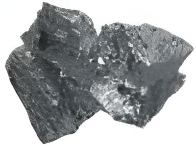 American Elements specializes in producing high purity Silicon Chunks using crystallization, solid state and other ultra high purification processes such as sublimation. Standard Chunk pieces are amorphous uniform pieces ranging in size from 5-15 mm. American Elements also casts any of the rare earth metals and most other advanced materials into granules, rod, bar or plate form We also produce Silicon as rod, pellets, powder, pieces, disc, ingot, wire, and in compound forms, such as oxide.
 The number of electrons in each of Silicon's shells is 2, 8, 4 and its electron configuration is [Ne] 3s2 3p2. The silicon atom has a radius of 111 pm and a Van der Waals radius of 210 pm. Silicon was discovered and first isolated by Jöns Jacob Berzelius in 1823. Silicon makes up 25.7% of the earth's crust, by weight, and is the second most abundant element, exceeded only by oxygen. The metalloid is rarely found in pure crystal form and is usually produced from the iron-silicon alloy ferrosilicon.
  Silica (or silicon dioxide), as sand, is a principal ingredient of glass, one of the most inexpensive of materials with excellent mechanical, optical, thermal, and electrical properties. Ultra high purity silicon can be doped with boron, gallium, phosphorus, or arsenic to produce silicon for use in transistors, solar cells, rectifiers, and other solid-state devices which are used extensively in the electronics industry.The name Silicon originates from the Latin word silex which means flint or hard stone.