Materials science has revolutionized the field of green technology, offering new processes, practices, sources of energy to power our lives that are more efficient and substantially decrease our impact on the environment.
High energy density lithium-ion (Li-I) batteries are the current hi-tech standard in the computing and electronics. The central mechanism by which the battery stores and generates energy is the reversible intercalation, or insertion, of lithium ions in the crystalline electrode materials; the positively-charged Li+ ions shuttling between the cathode (typically a lithium compound or mixed metal oxide) and the anode (typically graphitic carbon) through the electrolyte and separator membrane. 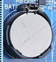 Because of the high reactivity of lithium metal with water, non-aqueous electrolyte formulations are required, typically lithium salts like LiPF6 in an organic solvent. Types of Li-ion batteries are known by their cathode materials, the most common being lithium cobalt oxide (LCO), lithium manganese oxide (LMO), lithium iron phosphate (LFP), and lithium nickel manganese cobalt oxide (NMC). Two other chemistries that are gaining attention for transportation and grid energy storage applications are lithium nickel cobalt aluminum oxide (NCA), used as a cathode, and lithium titanate (LTO), used as an anode material replacing graphite.
The current generation of lithium-ion batteries suffers from certain limitations to electrochemical performance that arise from its design, from the low conductivity of oxide-based cathode materials and insulating tendencies of electrolyte binders to the formation of dendrites at the surfaces of the electrode-electrolyte interface. Added to safety concerns based on the high reactivity of lithium metal, and the flammability and toxicity of electrolyte formulations, researchers are focusing on developing alternative designs that either improve existing lithium-ion technology or propose commercially viable alternative technologies. Some substitutes for electrode materials include lithium vanadium oxide and lithium vanadium phosphate.
Alternative chemistries to the lithium-ion paradigm include lithium-sulfur, sodium sulfur, sodium ion, lithium-air, nickel-lithium, and vanadium redox (flow) batteries. In addition many novel experimental battery designs are under investigation that rely on advanced materials like copper antimonide nanowires, tin oxide nanocrystals, vanadium dioxide ribbons paired with graphene, and carbon nanotubes.
As the global demand for green energy sources continues to rise, the advancement of fuel cell design plays a critical role in the development of viable alternatives to fossil fuel-based technologies for portable, stationary, and grid-scale power generation and storage. Unlike batteries, which generate power from internally-stored electrochemical energy, fuel cells require the continuous input of a hydrogen-based fuel source in order to produce electricity. Fuel cells possess the advantage of being able to operate indefinitely, in theory, and can be fully discharged without suffering voltage disruptions or degradation of internal components.
Solid oxide fuel cells (SOFCs) use all solid components: the most common design uses yttria stabilized zirconia as the electrolyte, nickel-ceramic composites (cermets) for anodes, and lanthanum strontium manganite for cathodes. The use of all solid materials is the key defining feature of these cells, as it allows for the development of cell designs that are incompatible with the use of liquid electrolytes. SOFCs can run on a variety of fuels, including hydrocarbons and pure hydrogen gas, and require high operating temperatures regardless of fuel type. The high temperature is necessary for the solid electrolyte to achieve high enough conductivity for optimal cell performance. Solid oxide fuel cells are currently being used or considered for use in auxilary power, electric power plant, and distributed generation applications.
Polymer electrolye membrane fuel cells (PEMFCs), also known as proton exchange membrane fuel cells, are a class of fuel cells being developed for both transportation and stationary applications. They are a lower temperature fuel cell and feature a special polymer membrane which serves as the electrolyte. The chemistry which produces the energy in all PEMFC cells is hydrogen-based, but some cell designs use hydrogen directly, while others are designed for use with hydrogen-heavy organic molecules. Advantages of PEMFC fuel cells include quick startup times, low operating temperature, and the durability and design advantages inherent to using a solid rather than liquid electrolyte. However, the catalysts they require make them expensive to build and they are sensitive to fuel impurities. Additionally, the low operating temperature of PEMFCs, while advantageous in some respects, does make using their waste heat to increase overall system efficiency impractical. PEMFCs are currently mostly of interest for transportation applications, or for short-term stationary applications, such as to serve as a backup power source.
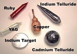
Photovoltaics constitute the fastest growing segment of the modern energy market, and for good reason. Photovoltaic systems are clean, produce electricity directly, and are scalable to meet the demands of a vast range of applications.  The most prominent materials used in the current generation of solar cells are Copper Indium Selenide (CIS)/Copper Indium Gallium Selenide (CIGS) and Cadmium Telluride (CdTe). Both cell types use the material they are named for as the p-type sunlight-absorbing layer, while cadmium sulfide is used as the n-type later. Both cell types boast significantly higher absorptivity than silicon, allowing for the use of much thinner material layers. However, technologies suffer from some issues with material toxicity and scarcity: cadmium is a toxic heavy metal, tellurium is as rare as gold, and indium is subject to supply problems related to the enormous demand for indium tin oxide for transparent electrodes.
While first and second generation solar cells typically use conventional semiconductor materials and designs dependent on single large-area p-n junctions to produce current, the next generation of solar technology uses radically different materials and cell designs for new approaches to lowering cost while maintaining reasonable cell efficiencies in addition to using more environmentally friendly materials. Polymer or organic photovoltaics (OPV) and dye-sensitized solar cells (DSSCs) are two promising candidates to become commercially viable alternatives to These cell types are of particular interest due to their ability to be fabricated very simply--the polymers lend themselves to roll-to-roll printing methods, allowing for extremely efficient and cheap production. Perovskite solar cells (PSCs) are another promising technology under development which uses perovskite-structured materials like hybrid organic-inorganic tin, cesium, or lead halides (such as methylammonium lead iodide). These cells possess the advantage of being simple and inexpensive to produce, while being tolerant to internal defects.
The old ways of "making stuff" pale in comparison to the efficiency of the newest method of creation--additive manufacturing, also known as 3D-printing. Once limited to building smaller objects using polymers, additive manufacturing now has an increasing range of source materials available such as from metal, alloy, and ceramic powders to construct large scale-objects layer-by-layer. The advantage of 3D printing is low volume production, conserving materials to fabricate only what is needed (known as "rapid prototyping"), thus conserving time and eliminating waste. Additive manufacturing can produce objects from advanced medical prostheses to aerospace and automotive parts; future applications may extend to the nanoscale, allowing for atomic level building.

From laser crystals to LEDs, advanced optical materials are ubiquitous in the field of high technology. Through materials science, the oldest and most well-known optical material, glass, can be made bulletproof, shatterproof, touch sensitive, electrically conductive, and responsive to fluctuations in light and temperature. Rare earth elements are particularly versatile in optical materials; cerium oxide is one of the most effective materials for precision polishing, and oxides of neodymium, praseodymium, and lanthanum are used to impart both colors and additional properties to glasses such as infrared absorption (used in night-vision goggles). The rare earths are also important dopants in laser crystals. Nd:YAG (neodymium-doped yttrium aluminum garnet) lasers are one of the most common types, used in dentistry, medicine, and defense, although YAG lasers can be doped with other rare earths including erbium, ytterbium, and thulium, or transition metals like chromium. Doping with different elements yields gain mediums that lase at different wavelengths, giving them applications as phosphors or scintillators. Light-emitting diodes (LEDs) are are solid-state lighting devices composed of semiconductors like Gallium Nitride (GaN) used in energy-efficient light bulbs and display screens for electronic devices like televisions and smartphones. Development is underway to produce LEDs from alternate materials to improve efficiency and performance, particularly brightness and color quality. Examples of next-generation types of LEDs are those that use organic semiconductors (OLEDs) and quantum dots (QLEDs).
The history of applying thin metallic coatings to surfaces spans hundreds of years, from the experiments of Thomas Edison and the rise of metal plating during World War II to the present. Now, the various techniques of the process known as thin film deposition are crucial to all fields of high technology including the fabrication of integrated circuits, semiconductor crystals, and nanomaterials. "Depositing" the thinnest layers of materials is achieved via physical or chemical methods including "sputtering," which involves controlled removal and conversion of the target material into a directed gaseous/plasma phase through ionic bombardment.

Materials science is the foundation of one of humanity's greatest achievements--space exploration. Outer space is the harshest imaginable environment, requiring materials that can withstand the intense heat of entering and exiting earth's atmosphere to the constant bombardment from solar radiation. Ultrawhite anti-reflective coatings created from high purity oxides, refractory structural alloys made from aluminum and beryllium that are both ultra strong and ultra light , and parts made from iridium (the lowest corroding metal known) have become the standard for constructing spacecraft and satellites.