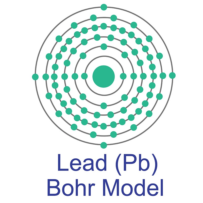
 See more Lead products. Lead (atomic symbol: Pb, atomic number: 82) is a Block P, Group 14, Period 6 element with an atomic radius of 207.2. The number of electrons in each of Lead's shells is [2, 8, 18, 32, 18, 4] and its electron configuration is [Xe] 4f14 5d10 6s2 6p2. The lead atom has a radius of 175 pm and a Van der Waals radius of 202 pm. In its elemental form, lead has a metallic gray appearance. Lead occurs naturally as a mixture of four stable isotopes: 204Pb (1.48%), 206Pb (23.6%), 207Pb (22.6%), and 208Pb (52.3%).
  Lead is obtained mainly from galena (PbS) by a roasting process. Anglesite, cerussite, and minim are other common lead containing minerals. Lead does occur as a free element in nature, but it is rare. It is a dense, soft metal that is very resistant to corrosion and poorly conductive compared to other metals. Its density and low melting point make it useful in applications such as electrolysis and industrial materials.
Materials
Materials by Form
2D Materials Alloy & Alloy Forms Pure Metals & Metal FormsCeramic FibersFoams: Metallic & Ceramic High Purity Materials Isotopes MXenesOxides Rare Earths Semiconductors Solutions
Chemicals & Salts
All Chemicals & Salts Acetates Aluminides Ammonium Sulfates Antimonides Arsenates Benzoate Bromates Bromides Carbonates Chlorides Chromates Fluorides Hydrides Hydroxides Iodates Iodides Lactates Molybdates Nitrates Oxalates Oxides Perchlorates Phosphates Selenates Selenides Selenites Silicates Stearates Sulfates Sulfides Sulfites Tantalates Tellurates Tellurides Tellurites ThiocyanatesVanadates
Ceramics
Nanomaterials
Organometallics
Materials by Application
Additive Manufacturing & 3D Printing Battery & Supercapacitor Materials Catalysts Dental Materials Electronics Materials Fuel Cell Materials Fusion EnergyGlass Manufacturing Green Technology & Alternative Energy Hydrogen Storage Laser Crystals Life Sciences & Biomaterials Metallurgy Nanotechnology & Nanomaterials Optical Materials Photovoltaic & Solar Energy Plating Pigments & Coatings Research & Development Space Technology Sputtering Targets Thin Film Deposition Water Treatment Weather Modification
Life Science Chemicals
Life Science Products AlcoholsAldehydesAmidesAminesAmino Acids & DerivativesAromaticsArylsAzetidinesBenzimidazolesBenzisoxazolesBenzodioxansBenzofuransBenzothiazolesBenzothiophenesBenzoxazolesCarboxylic AcidsEnzymes & InhibitorsEstersEthersFluorinated Building BlocksFuransHalidesImidazolesImidazolidinesIndazolesIndolesIndolinesIsoquinolinesIsoxazolesKetonesMorpholinesNaphthyridinesNitrilesOrganoboronOrganosiliconOxadiazolesOxazolesPharmaceuticals & IntermediatesPhenolsPhytochemicalsPiperazinesPiperidinesPyrazinesPyrazolesPyridazinesPyridinesPyrimidinesPyrrolesPyrrolidinesPyrrolinesQuinazolinesQuinolinesQuinoxalinesSpiroesSulfonyl ChloridesTetrahydroisoquinolinesTetrahydropyransTetrahydroquinolinesTetrazolesThiadiazolesThiazolesThiazolidinesThiolsThiophenesTriazinesTriazoles
About Us
Locations
Austria Belgium Brazil Canada China & Hong Kong Czech Republic Denmark Finland France Germany Greece Hungary India Indonesia Israel Italy Japan Malaysia Mexico Netherlands Norway Philippines Poland Portugal Russia Singapore South Korea Spain Sweden Switzerland Taiwan Thailand Turkey United Kingdom United States
Industries
Aerospace Agriculture Automotive Chemical Manufacturing Defense Dentistry Electronics Energy Storage & Batteries Fine Art Materials Fuel CellsFusion Energy Glass Investment Grade Metals Jewelry & Fashion Lasers Lighting Medical Devices Museums & Galleries Nuclear Energy Oil & Gas Optics Paper & Pulp Pharmaceuticals & Cosmetics Research & Laboratory Robotics Solar Energy Space Sports Equipment Steel & Alloy Producers Textiles & Fabrics Water Treatment Municipalities
Follow Us
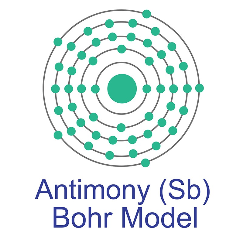
 The most common source of antimony is the