SECTION 1. IDENTIFICATION
Product Name: Calcium Silicate Sputtering Target
Product Number: All applicable American Elements product codes, e.g. CA-SIAT-02-ST
, CA-SIAT-025-ST
, CA-SIAT-03-ST
, CA-SIAT-035-ST
, CA-SIAT-04-ST
, CA-SIAT-05-ST
CAS #: 1344-95-2
Relevant identified uses of the substance: Scientific research and development
Supplier details:
American Elements
10884 Weyburn Ave.
Los Angeles, CA 90024
Tel: +1 310-208-0551
Fax: +1 310-208-0351
Emergency telephone number:
Domestic, North America: +1 800-424-9300
International: +1 703-527-3887
SECTION 2. HAZARDS IDENTIFICATION
Classification of the substance or mixture
GHS Classification in accordance with 29 CFR 1910 (OSHA HCS)
Eye irritation(Category 2A), H319
Specific target organ toxicity -single exposure(Category 3), Respiratory system, H335
GHS Label elements, including precautionary statements
Pictogram

Signal word
Warning
Hazard statement(s)
H319
Causes serious eye irritation.
H335
May cause respiratory irritation.
Precautionary statement(s)
P261
Avoid breathing dust/ fume/ gas/ mist/ Vapors/ spray.
P264
Wash skin thoroughly after handling.
P271
Use only outdoors or in a well-ventilated area.
P280
Wear protective gloves/ eye protection/ face protection.
P304 + P340
IF INHALED: Remove victim to fresh air and keep at rest in a position comfortable for breathing.
P305 + P351 + P338
IF IN EYES: Rinse cautiously with water for several minutes. Remove contact lenses, if present and easy to do. Continue rinsing.
P312
Call a POISON CENTER or doctor/ physician if you feel unwell.
P337 + P313
If eye irritation persists: Get medical advice/ attention.
P403 + P233
Store in a well-ventilated place. Keep container tightly closed.
P405
Store locked up.
P501
Dispose of contents/ container to an approved waste disposal plant.
Hazards not otherwise classified (HNOC) or not covered by GHS-none
SECTION 3. COMPOSITION/INFORMATION ON INGREDIENTS
Substances
Synonyms:
Calcium metasilicate
Calcium silicon oxide
Silicon calcium oxide
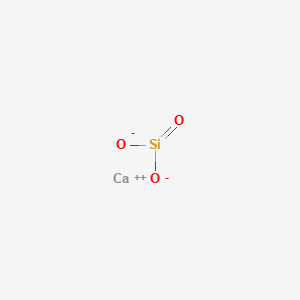
Formula: CaO3Si
Molecular Weight: 116.16 g/mol
CAS-No.: 1344-95-2
EC-No.: 233-250-6
Component
Calcium silicate
Classification
Eye Irrit.2A; STOT SE3; H319, H335
Concentration
-
SECTION 4. FIRST AID MEASURES
Description of first aid measures
General advice
Consult a physician. Show this safety data sheet to the doctor in attendance.
Move out of dangerous area.
If inhaled
If breathed in, move person into fresh air. If not breathing, give artificial respiration. Consult a physician.
In case of skin contact
Wash off with soap and plenty of water. Consult a physician.
In case of eye contact
Rinse thoroughly with plenty of water for at least 15 minutes and consult a physician.
If swallowed
Never give anything by mouth to an unconscious person. Rinse mouth with water. Consult a physician.
Most important symptoms and effects, both acute and delayed
The most important known symptoms and effects are described in the labelling (see section 2) and/or in section 11
Indication of any immediate medical attention and special treatment needed
no data available
SECTION 5. FIREFIGHTING MEASURES
Extinguishing media
Suitable extinguishing media
Use water spray, alcohol-resistant foam, dry chemical or carbon dioxide.
Special hazards arising from the substance or mixture
Calcium oxide, silicon oxides
Advice for firefighters
Wear self contained breathing apparatus for fire fighting if necessary.
Further information
no data available
SECTION 6. ACCIDENTAL RELEASE MEASURES
Personal precautions, protective equipment and emergency procedures
Use personal protective equipment. Avoid dust formation. Avoid breathing Vapors, mist or gas. Ensure adequate ventilation. Evacuate personnel to safe areas. Avoid breathing dust.
For personal protection see section 8.
Environmental precautions
Do not let product enter drains.
Methods and materials for containment and cleaning up
Pick up and arrange disposal without creating dust. Sweep up and shovel. Keep in suitable, closed containers for disposal.
Reference to other sections
For disposal see section 13.
SECTION 7. HANDLING AND STORAGE
Precautions for safe handling
Avoid contact with skin and eyes. Avoid formation of dust and aerosols.
Provide appropriate exhaust ventilation at places where dust is formed.Normal measures for preventive fire protection.
For precautions see section 2.
Conditions for safe storage, including any incompatibilities
Keep container tightly closed in a dry and well-ventilated place.
Specific end use(s)
Apart from the uses mentioned in section 1 no other specific uses are stipulated
SECTION 8. EXPOSURE CONTROLS/PERSONAL PROTECTION
Control parameters
Components with workplace control parameters
Contains no substances with occupational exposure limit values.
Exposure controls
Appropriate engineering controls
Handle in accordance with good industrial hygiene and safety practice. Wash hands before breaks and at the end of workday.
Personal protective equipment
Eye/face protection
Safety glasses with side-shields conforming to EN166 Use equipment for eye protecti
on tested and approved under appropriate government standards such as NIOSH (US) or EN 166(EU).
Skin protection
Handle with gloves. Gloves must be inspected prior to use. Use proper glove removal technique (without touching glove's outer surface) to avoid skin contact with this product. Dispose of contaminated gloves after use in accordance with applicable laws and good laboratory practices. Wash and dry hands.
Body Protection
impervious clothing, The type of protective equipment must be selected according
to the concentration and amount of the dangerous substance at the specific workplace.
Respiratory protection
For nuisance exposures use type P95 (US) or type P1 (EU EN 143) particle respirator.For higher level protection use type OV/AG/P99 (US) or type ABEK-P2 (EU EN 143) respirator cartridges. Use respirators and components tested and approved under appropriate government standards such as NIOSH (US) or CEN (EU).
Control of environmental exposure
Do not let product enter drains.
SECTION 9. PHYSICAL AND CHEMICAL PROPERTIES
Appearance
Form: solid
Odor
no data available
Odor Threshold
no data available
pH
no data available
Melting point/freezing point
no data available
Initial boiling point and boiling range
no data available
Flash point
not applicable
EVaporation rate
no data available
Flammability (solid, gas)
no data available
Upper/lower flammability or explosive limits
no data available
Vapor pressure
no data available
Vapor density
no data available
Relative density
2.900 g/cm3
Water solubility
no data available
Partition coefficient: n-octanol/water
no data available
Auto-ignition temperature
no data available
Decomposition temperature
no data available
Viscosity
no data available
Explosive properties
no data available
Oxidizing properties
no data available
Other safety information
no data available
SECTION 10. STABILITY AND REACTIVITY
Reactivity
no data available
Chemical stability
Stable under recommended storage conditions.
Possibility of hazardous reactions
no data available
Conditions to avoid
no data available
Incompatible materials
Strong oxidizing agents
Hazardous decomposition products
Other decomposition products-no data available
In the event of fire: see section 5
SECTION 11. TOXICOLOGICAL INFORMATION
Information on toxicological effects
Acute toxicity
no data available
Dermal:
no data available
Skin corrosion/irritation
no data available
Serious eye damage/eye irritation
no data available
Respiratory or skin sensitisation
no data available
Germ cell mutagenicity
no data available
Carcinogenicity
IARC:
No component of this product present at levels greater than or equal to 0.1% is identified as
probable, possible or confirmed human carcinogen by IARC.
ACGIH:
No component of this product present at levels greater than or equal to 0.1% is identified as a
carcinogen or potential carcinogen by ACGIH.
NTP:
No component of this product present at levels greater than or equal to 0.1% is identified as a
known or anticipated carcinogen by NTP.
OSHA:
No component of this product present at levels greater than or equal to 0.1% is identified as a
carcinogen or potential carcinogen by OSHA.
Reproductive toxicity
no data available
Specific target organ toxicity -single exposure
Inhalation-May cause respiratory irritation.
Specific target organ toxicity -repeated exposure
no data available
Aspiration hazard
no data available
Additional Information
RTECS: VV9170000
To the best of our knowledge, the chemical, physical, and toxicological properties have not been thoroughly investigated.
SECTION 12. ECOLOGICAL INFORMATION
Toxicity
no data available
Persistence and degradability
no data available
Bioaccumulative potential
no data available
Mobility in soil
no data available
Results of PBT and vPvB assessment
PBT/vPvB assessment not available as chemical safety assessment not required/not conducted
Other adverse effects
no data available
SECTION 13. DISPOSAL CONSIDERATIONS
Waste treatment methods
Product
Offer surplus and non-recyclable solutions to a licensed disposal company.
Contact a licensed professional waste disposal service to dispose of this material.
Contaminated packaging
Dispose of as unused product.
SECTION 14. TRANSPORT INFORMATION
DOT (US)
Not dangerous goods
IMDG
Not dangerous goods
IATA
Not dangerous goods
SECTION 15. REGULATORY INFORMATION
SARA 302 Components
SARA 302: No chemicals in this material are subject to the reporting requirements of SARA Title III, Section 302.
SARA 313 Components
SARA 313: This material does not contain any chemical components with known CAS numbers that exceed the threshold (De Minimis) reporting levels established by SARA Title III, Section 313.
SARA 311/312 Hazards
Acute Health Hazard
Massachusetts Right To Know Components
No components are subject to the Massachusetts Right to Know Act.
Pennsylvania Right To Know Components
Calcium silicate
CAS-No.
1344-95-2
Revision Date
New Jersey Right To Know Components
Calcium silicate
CAS-No.
1344-95-2
California Prop. 65 Components
This product does not contain any chemicals known to State of California to cause cancer, birth defects, or any other reproductive harm.
SECTION 16. OTHER INFORMATION
Safety Data Sheet according to Regulation (EC) No. 1907/2006 (REACH). The above information is believed to be correct but does not purport to be all inclusive and shall be used only as a guide. The information in this document is based on the present state of our knowledge and is applicable to the product with regard to appropriate safety precautions. It does not represent any guarantee of the properties of the product. American Elements shall not be held liable for any damage resulting from handling or from contact with the above product. See reverse side of invoice or packing slip for additional terms and conditions of sale. COPYRIGHT 1997-2022 AMERICAN ELEMENTS. LICENSED GRANTED TO MAKE UNLIMITED PAPER COPIES FOR INTERNAL USE ONLY.
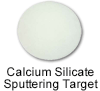 American Elements specializes in producing high purity Calcium Silicate Sputtering Targets with the highest possible density and smallest possible average grain sizes for use in semiconductor, chemical vapor deposition (CVD) and physical vapor deposition (PVD) display and optical applications. Our standard Sputtering Targets for thin film are available monoblock or bonded with planar target dimensions and configurations up to 820 mm with hole drill locations and threading, beveling, grooves and backing designed to work with both older sputtering devices as well as the latest process equipment, such as large area coating for solar energy or fuel cells and flip-chip applications. Research sized targets are also produced as well as custom sizes and alloys. All targets are analyzed using best demonstrated techniques including X-Ray Fluorescence (XRF), Glow Discharge Mass Spectrometry (GDMS), and Inductively Coupled Plasma (ICP). "Sputtering" allows for thin film deposition of an ultra high purity sputtering metallic or oxide material onto another solid substrate by the controlled removal and conversion of the target material into a directed gaseous/plasma phase through ionic bombardment. Materials are produced using crystallization, solid state and other ultra high purification processes such as sublimation. American Elements specializes in producing custom compositions for commercial and research applications and for new proprietary technologies. American Elements also casts any of the rare earth metals and most other advanced materials into rod, bar or plate form, as well as other machined shapes and through other processes such as nanoparticles and in the form of solutions and organometallics. We also produce Calcium as disc, granules, ingot, pellets, pieces, powder, and rod. Other shapes are available by request.
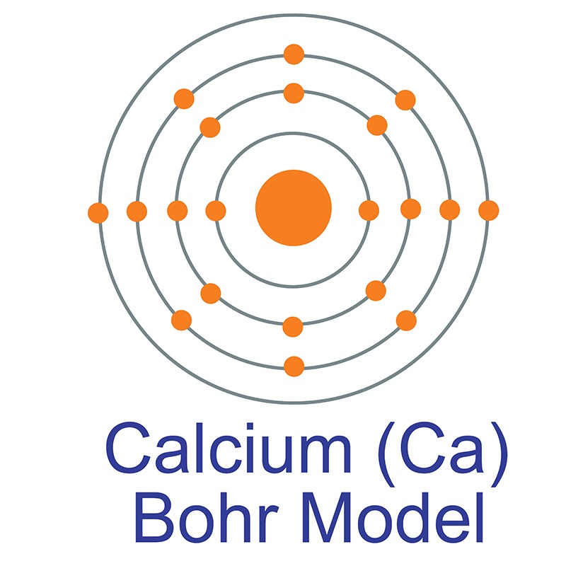 The calcium atom has a radius of 197 pm and a Van der Waals radius of 231 pm. Calcium was discovered and first isolated by Sir Humphrey Davy in 1808. It is the fifth most abundant element in the earth's crust and can be found in minerals such as dolomite, gypsum, plagioclases, amphiboles, pyroxenes and garnets. In its elemental form, calcium has a dull gray-silver appearance. Calcium is a reactive, soft metal that is a member of the alkaline earth elements.
 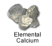 It frequently serves as an alloying agent for other metals like aluminum and beryllium, and industrial materials like cement and mortar are composed of calcium compounds like calcium carbonate. It is also an biologically essential substance found in teeth, bones, and shells. The name "calcium" originates from the Latin word "calics," meaning lime.
 The number of electrons in each of Silicon's shells is 2, 8, 4 and its electron configuration is [Ne] 3s2 3p2. The silicon atom has a radius of 111 pm and a Van der Waals radius of 210 pm. Silicon was discovered and first isolated by Jöns Jacob Berzelius in 1823. Silicon makes up 25.7% of the earth's crust, by weight, and is the second most abundant element, exceeded only by oxygen. The metalloid is rarely found in pure crystal form and is usually produced from the iron-silicon alloy ferrosilicon.
  Silica (or