SECTION 1. IDENTIFICATION
Product Name: Silver Selenide
Product Number: All applicable American Elements product codes, e.g. AG-SE-05-I
, AG-SE-05-L
, AG-SE-05-P
, AG-SE-05-ST
, AG-SE-05-WF
CAS #: 1302-09-6
Relevant identified uses of the substance: Scientific research and development
Supplier details:
American Elements
10884 Weyburn Ave.
Los Angeles, CA 90024
Tel: +1 310-208-0551
Fax: +1 310-208-0351
Emergency telephone number:
Domestic, North America: +1 800-424-9300
International: +1 703-527-3887
SECTION 2. HAZARDS IDENTIFICATION
2.1 Classification of the substance or mixture
GHS Classification in accordance with 29 CFR 1910 (OSHA HCS)
Acute toxicity, Oral (Category 3), H301
Acute toxicity, Inhalation (Category 4), H332
2.2 GHS Label elements, including precautionary statements
Pictogram
Signal word Danger
Hazard statement(s)
H301 Toxic if swallowed.
H332 Harmful if inhaled.
Precautionary statement(s)
P261 Avoid breathing dust/ fume/ gas/ mist/ Vapors/ spray.
P264 Wash skin thoroughly after handling.
P270 Do not eat, drink or smoke when using this product.
P271 Use only outdoors or in a well-ventilated area.
P301 + P310 + P330 IF SWALLOWED: Immediately call a POISON CENTER or doctor/
physician. Rinse mouth.
P304 + P340 + P312 IF INHALED: Remove victim to fresh air and keep at rest in a position
comfortable for breathing. Call a POISON CENTER or doctor/ physician if
P405 Store locked up.
P501 Dispose of contents/ container to an approved waste disposal plant.
2.3 Hazards not otherwise classified (HNOC) or not covered by GHS - none
SECTION 3. COMPOSITION/INFORMATION ON INGREDIENTS
3.1 Substances
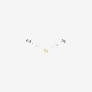
Formula : Ag2Se
Molecular weight : 294.7 g/mol
CAS-No. : 1302-09-6
EC-No. : 215-099-8
Index-No. : 034-002-00-8
Hazardous components
Component Classification Concentration
Silver(I) selenide
Acute Tox. 3; Acute Tox. 4;
H301, H332
<= 100 %
SECTION 4. FIRST AID MEASURES
4.1 Description of first aid measures
General advice
Consult a physician. Show this safety data sheet to the doctor in attendance.Move out of dangerous area.
If inhaled
If breathed in, move person into fresh air. If not breathing, give artificial respiration. Consult a physician.
In case of skin contact
Wash off with soap and plenty of water. Take victim immediately to hospital. Consult a physician.
In case of eye contact
Flush eyes with water as a precaution.
If swallowed
Never give anything by mouth to an unconscious person. Rinse mouth with water. Consult a physician.
4.2 Most important symptoms and effects, both acute and delayed
The most important known symptoms and effects are described in the labelling (see section 2.2) and/or in section 11
4.3 Indication of any immediate medical attention and special treatment needed
No data available
SECTION 5. FIREFIGHTING MEASURES
5.1 Extinguishing media
Suitable extinguishing media
Use water spray, alcohol-resistant foam, dry chemical or carbon dioxide.
5.2 Special hazards arising from the substance or mixture
Silver/silver oxides, Selenium/selenium oxides
5.3 Advice for firefighters
Wear self-contained breathing apparatus for firefighting if necessary.
5.4 Further information
No data available
SECTION 6. ACCIDENTAL RELEASE MEASURES
6.1 Personal precautions, protective equipment and emergency procedures
Wear respiratory protection. Avoid dust formation. Avoid breathing Vapors, mist or gas. Ensure adequate ventilation.
Evacuate personnel to safe areas. Avoid breathing dust.
For personal protection see section 8.
6.2 Environmental precautions
Prevent further leakage or spillage if safe to do so. Do not let product enter drains.
6.3 Methods and materials for containment and cleaning up
Pick up and arrange disposal without creating dust. Sweep up and shovel. Keep in suitable, closed containers for
disposal.
6.4 Reference to other sections
For disposal see section 13.
SECTION 7. HANDLING AND STORAGE
7.1 Precautions for safe handling
Avoid contact with skin and eyes. Avoid formation of dust and aerosols.Further processing of solid materials may result
in the formation of combustible dusts. The potential for combustible dust formation should be taken into consideration
before additional processing occurs.
Provide appropriate exhaust ventilation at places where dust is formed.
For precautions see section 2.2.
7.2 Conditions for safe storage, including any incompatibilities
Keep container tightly closed in a dry and well-ventilated place.
Moisture sensitive.
Storage class (TRGS 510): Non-combustible, acute toxic Cat. 1 and 2 / very toxic hazardous materials
7.3 Specific end use(s)
Apart from the uses mentioned in section 1.2 no other specific uses are stipulated
SECTION 8. EXPOSURE CONTROLS/PERSONAL PROTECTION
8.1 Control parameters
Components with workplace control parameters
Component CAS-No. Value Control
parameters
Basis
Silver(I) selenide 1302-09-6 TWA 0.200000
mg/m3
USA. ACGIH Threshold Limit Values
(TLV)
Remarks Upper Respiratory Tract irritation
Eye irritation
TWA 0.200000
mg/m3
USA. Occupational Exposure Limits
(OSHA) - Table Z-1 Limits for Air
Contaminants
TWA 0.200000
mg/m3
USA. NIOSH Recommended
Exposure Limits
TWA 0.2 mg/m3 USA. Occupational Exposure Limits
(OSHA) - Table Z-1 Limits for Air
Contaminants
TWA 0.2 mg/m3 USA. ACGIH Threshold Limit Values
(TLV)
Upper Respiratory Tract irritation
Eye irritation
TWA 0.2 mg/m3 USA. NIOSH Recommended
Exposure Limits
8.2 Exposure controls
Appropriate engineering controls
Avoid contact with skin, eyes and clothing. Wash hands before breaks and immediately after handling the product.
Personal protective equipment
Eye/face protection
Face shield and safety glasses Use equipment for eye protection tested and approved under appropriate
government standards such as NIOSH (US) or EN 166(EU).
Skin protection
Handle with gloves. Gloves must be inspected prior to use. Use proper glove removal technique (without
touching glove's outer surface) to avoid skin contact with this product. Dispose of contaminated gloves after
use in accordance with applicable laws and good laboratory practices. Wash and dry hands.
Body Protection
Complete suit protecting against chemicals, The type of protective equipment must be selected according to
the concentration and amount of the dangerous substance at the specific workplace.
Respiratory protection
Where risk assessment shows air-purifying respirators are appropriate use a full-face particle respirator type
N99 (US) or type P2 (EN 143) respirator cartridges as a backup to engineering controls. If the respirator is the
sole means of protection, use a full-face supplied air respirator. Use respirators and components tested and
approved under appropriate government standards such as NIOSH (US) or CEN (EU).
Control of environmental exposure
Prevent further leakage or spillage if safe to do so. Do not let product enter drains.
SECTION 9. PHYSICAL AND CHEMICAL PROPERTIES
9.1 Information on basic physical and chemical properties
a) Appearance Form: solid
b) Odor No data available
c) Odor Threshold No data available
d) pH No data available
e) Melting point/freezing
point
No data available
f) Initial boiling point and
boiling range
No data available
g) Flash point N/A
h) Evaporation rate No data available
i) Flammability (solid, gas) No data available
j) Upper/lower
flammability or
explosive limits
No data available
k) Vapor pressure No data available
l) Vapor density No data available
m) Relative density 8.22 g/cm3 at 25 °C (77 °F)
n) Water solubility No data available
o) Partition coefficient: noctanol/
water
No data available
p) Auto-ignition
temperature
No data available
q) Decomposition
temperature
No data available
r) Viscosity No data available
s) Explosive properties No data available
t) Oxidizing properties No data available
9.2 Other safety information
No data available
SECTION 10. STABILITY AND REACTIVITY
10.1 Reactivity
No data available
10.2 Chemical stability
Stable under recommended storage conditions.
10.3 Possibility of hazardous reactions
No data available
10.4 Conditions to avoid
Avoid moisture.
10.5 Incompatible materials
Strong oxidizing agents
10.6 Hazardous decomposition products
Other decomposition products - No data available
In the event of fire: see section 5
SECTION 11. TOXICOLOGICAL INFORMATION
11.1 Information on toxicological effects
Acute toxicity
No data available
Dermal: No data available
No data available
Skin corrosion/irritation
No data available
Serious eye damage/eye irritation
No data available
Respiratory or skin sensitisation
No data available
Germ cell mutagenicity
No data available
Carcinogenicity
IARC: 3 - Group 3: Not classifiable as to its carcinogenicity to humans (Silver(I) selenide)
NTP: No component of this product present at levels greater than or equal to 0.1% is identified as a
known or anticipated carcinogen by NTP.
OSHA: No component of this product present at levels greater than or equal to 0.1% is identified as a
carcinogen or potential carcinogen by OSHA.
Reproductive toxicity
No data available
No data available
Specific target organ toxicity - single exposure
No data available
Specific target organ toxicity - repeated exposure
No data available
Aspiration hazard
No data available
Additional Information
RTECS: Not available
Acute selenium poisoning produces central nervous system effects, which include nervousness, convulsions, and
drowsiness. Other signs of intoxication can include skin eruptions, lassitude, gastrointestinal distress, teeth that are
discolored or decayed, odorous ("garlic") breath, and partial loss of hair and nails. Chronic exposure by inhalation can
produce symptoms that include pallor, coating of the tongue, anemia, irritation of the mucosa, lumbar pain, liver and
spleen damage, as well as any of the other previously mentioned symptoms. Chronic contact with selenium
compounds may cause garlic odor of breath and sweat, dermatitis, and moderate emotional instability., Gastrointestinal
disturbance, Dizziness, Nausea, Headache, Vomiting, Diarrhoea, Abdominal pain, May cause argyria (a slate-gray or
bluish discoloration of the skin and deep tissues due to the deposit of insoluble albuminate of silver)., To the best of our
knowledge, the chemical, physical, and toxicological properties have not been thoroughly investigated.
Stomach - Irregularities - Based on Human Evidence
Stomach - Irregularities - Based on Human Evidence
SECTION 12. ECOLOGICAL INFORMATION
12.1 Toxicity
No data available
12.2 Persistence and degradability
No data available
12.3 Bioaccumulative potential
No data available
12.4 Mobility in soil
No data available
12.5 Results of PBT and vPvB assessment
PBT/vPvB assessment not available as chemical safety assessment not required/not conducted
12.6 Other adverse effects
SECTION 13. DISPOSAL CONSIDERATIONS
13.1 Waste treatment methods
Product
Offer surplus and non-recyclable solutions to a licensed disposal company. Contact a licensed professional waste
disposal service to dispose of this material. Dissolve or mix the material with a combustible solvent and burn in a
chemical incinerator equipped with an afterburner and scrubber.
Contaminated packaging
Dispose of as unused product.
SECTION 14. TRANSPORT INFORMATION
DOT (US)
UN number: 3283 Class: 6.1 Packing group: II
Proper shipping name: Selenium compound, solid, n.o.s. (Silver(I) selenide)
Reportable Quantity (RQ):
Poison Inhalation Hazard: No
IMDG
UN number: 3283 Class: 6.1 Packing group: II EMS-No: F-A, S-A
Proper shipping name: SELENIUM COMPOUND, SOLID, N.O.S. (Silver(I) selenide)
IATA
UN number: 3283 Class: 6.1 Packing group: II
Proper shipping name: Selenium compound, solid, n.o.s. (Silver(I) selenide)
SECTION 15. REGULATORY INFORMATION
SARA 302 Components
Aldrich - 400637 Page 7 of 7
No chemicals in this material are subject to the reporting requirements of SARA Title III, Section 302.
SARA 313 Components
The following components are subject to reporting levels established by SARA Title III, Section 313:
Silver(I) selenide
CAS-No.
1302-09-6
Revision Date
2007-07-01
SARA 311/312 Hazards
Acute Health Hazard, Chronic Health Hazard
Massachusetts Right To Know Components
No components are subject to the Massachusetts Right to Know Act.
Pennsylvania Right To Know Components
Silver(I) selenide
CAS-No.
1302-09-6
Revision Date
2007-07-01
New Jersey Right To Know Components
Silver(I) selenide
CAS-No.
1302-09-6
Revision Date
2007-07-01
California Prop. 65 Components
This product does not contain any chemicals known to State of California to cause cancer, birth defects, or any other
reproductive harm.
SECTION 16. OTHER INFORMATION
Safety Data Sheet according to Regulation (EC) No. 1907/2006 (REACH). The above information is believed to be correct but does not purport to be all inclusive and shall be used only as a guide. The information in this document is based on the present state of our knowledge and is applicable to the product with regard to appropriate safety precautions. It does not represent any guarantee of the properties of the product. American Elements shall not be held liable for any damage resulting from handling or from contact with the above product. See reverse side of invoice or packing slip for additional terms and conditions of sale. COPYRIGHT 1997-2022 AMERICAN ELEMENTS. LICENSED GRANTED TO MAKE UNLIMITED PAPER COPIES FOR INTERNAL USE ONLY.
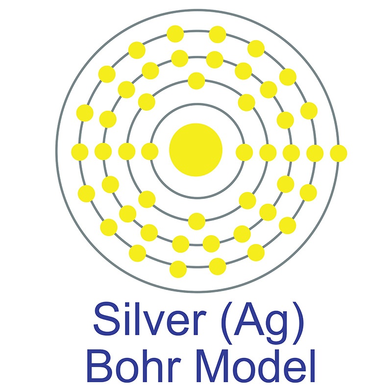 The number of electrons in each of Silver's shells is 2, 8, 18, 18, 1 and its electron configuration is [Kr]4d10 5s1. The silver atom has a radius of 144 pm and a Van der Waals radius of 203 pm. Silver was first discovered by Early Man prior to 5000 BC. In its elemental form, silver has a brilliant white metallic luster.
  It is a little harder than gold and is very ductile and malleable, being exceeded only by gold and perhaps palladium. Pure silver has the highest electrical and thermal conductivity of all metals and possesses the lowest contact resistance. It is stable in pure air and water, but tarnishes when exposed to ozone, hydrogen sulfide, or air containing sulfur. It is found in copper, copper-nickel, lead, and lead-zinc ores, among others. Silver was named after the Anglo-Saxon word "seolfor" or "siolfur," meaning 'silver'.
 See more Selenium products.
 One of the most common uses for selenium is in