Photovoltaic & Solar Energy Materials
The enormous promise of solar energy has long been known: every hour, enough energy to meet worldwide annual energy demands reaches earth’s surface in the form of solar radiation. It is only in recent years, however, that we have even begun to scratch the surface of what is possible in solar energy harvesting technology. The energy of solar radiation can be captured in a useful form as electrical, thermal, or chemical energy depending on the technology used, and American Elements is committed to supporting the development and continual improvement of all solar technologies.
#3: First Solar Builds Next-Generation Solar Panels Using American Elements Cadmium Selenide
Photovoltaics
Photovoltaics constitute the fastest growing segment of the modern energy market, and for good reason. Photovoltaic systems are clean, produce electricity directly, and are scalable to meet the demands of a vast range of applications.
Solar cell basics
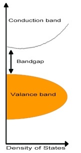
The natural phenomena underlying the function of these devices is the photovoltaic effect, in which electrons in a material are elevated from their valence band to the conduction band following the absorption of photons. The place previously occupied by the electron--which can also be called a negative charge carrier--becomes a positive charge carrier called a hole. Electrons from other atoms can then move into this hole, leaving holes of their own, and allowing the movement of charge through the material. In this way, a current can be produced in response to the absorption of energy from incident light.
Semiconductor materials may be produced to be intrinsically n-type, and have an excess of electrons or p-type, having an excess of holes, due to the elemental composition and crystalline structure of the material. When these two types of material are in contact with one another, they produce an electrical field in the area of the p-n junction. As photons elevate electrons in the material to the conduction band, the electron and the newly created hole--also referred to as negative and positive charge carriers, respectively--are pulled away from the junction in opposite directions due to the influence of this field. Collections circuits attached from the n-type layer to the p-type layer allow the electrons to go the long way around to ultimately recombine with the holes in the p-type layer, and energy in the form of electricity is collected from the flow of electrons through this external circuit.
The energetic difference between the valence and conduction bands is termed the bandgap, and is a physical property related to the composition of the material. The bandgap is important in photovoltaic devices because it describes the energy a photon must have in order to elevate an electron from the valence to the conduction band, as well as the maximum amount of energy that can be absorbed per photon in that material: photons with energies less than the bandgap will fail to be absorbed, while energy exceeding the bandgap is lost as heat, and thus not converted to electrical energy. Solar cells with a single p-n junction are therefore subject to the Shockley-Queisser limit--a theoretical maximum percentage of energy a cell with a given bandgap is capable of extracting from the total amount of energy in the incident light. The theoretical maximum efficiency of an ideal solar cell--with the ideal bandgap of 1.34eV--is about 33.7%, while the maximum efficiency of a silicon cell--with a less favorable bandgap of 1.1ev--is about 29.4%. The Shockley-Queisser limit can be surpassed through the use of multijunction cells that layer materials with smaller band gaps on top of those with larger bandgaps, allowing for the capture of energy from a wider range of photons, but efficiency gains must be balanced with increased production costs.
First and second generation photovoltaics
The first commercial solar cells produced used crystalline silicon, doped such that one side of the material is p-type and the other is n-type. Silicon is a well-studied, abundant material, and the semiconductor industry has ensured that the high-purity silicon necessary for solar cells is widely available, and therefore crystalline silicon cells still dominate the photovoltaic market today.
However, silicon is a relatively poor absorber of sunlight due to its indirect bandgap. This, along with the production techniques used to produce high-quality silicon crystals, necessitates the use of relatively thick layers of material to produce a functional solar cell, and the single-crystal silicon material used in the most efficient cells--which have a maximum efficiency of around 25%--is very expensive to produce. The cost of crystalline silicon cells can be lowered through the use of various forms of polycrystalline silicon, but this comes at the cost of lowering efficiency to 14-20%.
Another single-crystal material, gallium arsenide, has a closer-to-ideal bandgap and better absorptivity than silicon, which allowed for the production of high-efficiency solar cells even in the earliest days of photovoltaic technology. However, gallium arsenide cells are very expensive to produce, and historically have been used primarily in specialty applications, such as providing power for satellites.
The second generation of commercialized photovoltaic technology primarily uses alternative materials that could allow for production of thin-film solar cells. Thin film designs require less expensive semiconductor material, use adaptable thin-film deposition techniques for fabrication, and can use lightweight and even flexible substrate materials.
The most prominent of these designs are Copper Indium Selenide (CIS)/Copper Indium Gallium Selenide (CIGS) and Cadmium Telluride (CdTe) solar cells. Both cell types use the material they are named for as the p-type sunlight-absorbing layer, while cadmium sulfide is used as the n-type later. Both cell types boast significantly higher absorptivity than silicon, allowing for the use of much thinner material layers. These cells have yet to reach the efficiencies achieved with single-crystal silicon--their maximum efficiencies are around 20%--but the lower costs and design possibilities related to their thin-film structure have led to their their commercialization. CIGS development has lagged behind CdTe technology: the latter has gained significant market share since its recent commercialization, while companies utilizing CIGS technology have only recently begun large-scale production. Both technologies suffer from some problems with material toxicity and scarcity: cadmium is a toxic heavy metal, tellurium is as rare as gold, and indium is subject to supply problems related to the enormous demand for indium tin oxide for transparent electrodes. This has provoked research interest in a material with similar properties to CIGS,
Additionally, first-generation photovoltaic materials can now be produced in different forms for use in thin-film solar cells. Silicon can be used in thin-film cells as amorphous silicon (a-silicon) or extremely tiny silicon crystals (micro- or nanocrystalline silicon). These cells have poor efficiency compared to typical silicon cells, but are relatively low-cost, and were initially used to power cheap electronic devices that required very little power, such as pocket calculators. Recently various design innovations have been developed to compensate for some of the limitations of thin-film silicon materials, allowing for development of some thin-film silicon cells for large-area applications, though even the best of these cells have lower efficiencies than other thin-film technologies. Gallium arsenide thin film cells have set efficiency records for single-junction thin-film cells, but are still usually more expensive than competing technologies. Gallium arsenide may additionally be combined with other gallium semiconductors to produce materials with a range of bandgaps, which is useful for the production of multijunction solar cells, which boast the highest solar cell efficiencies ever achieved. However, the additional production costs associated with these cells has limited their use primarily to applications where power-to-weight ratio is paramount--as in satellites--and to concentrator systems, where lenses or mirrors focus sunlight from large areas onto small solar cells to take maximum advantage of high-efficiencies.
First and second generation solar cell development has primarily sought to make solar energy cost-effective by producing single p-n junction cells that operated with efficiency as close to the Shockley-Queisser limit as possible while limiting costs of production. Efforts to improve the cost-effectiveness of these cells have focused on improving production techniques to allow for lower cost or better material properties, as well as the improvement of some cell-design elements to reduce losses due to reflected light (using anti-reflective surface treatments) and shading from surface electrical contacts (using altered metal contact designs or transparent conducting materials). Thin-film cells in particular remain relatively new commercial technologies with substantial room for continued efficiency improvements and cost reduction.
Next generation photovoltaics
While first and second generation solar cells typically use conventional semiconductor materials and designs dependent on single large-area p-n junctions to produce current, the next generation of solar technology uses radically different materials and cell designs for new approaches to lowering cost while maintaining reasonable cell efficiencies. Currently third-generation designs have yet to reach efficiencies already possible with commercially-available first and second generation photovoltaics, but development is ongoing.
The Grätzel Cell
In conventional photovoltaic devices, both the absorption of a photon to produce an electron-hole pair and the separation of those charges to produce current are achieved within the same material. An alternate photovoltaic device structure known as a Grätzel cell separates these processes, using one material to absorb photons to produce electron-hole pairs, while a wide-bandgap semiconductor, most often titanium oxide, separates the charges by carrying away the freed electrons. A third material, an electrolyte, then donates electrons to fill the hole left in the original dye molecule, which can then be re-excited by a new photon. These materials are all in intimate contact, as the semiconductor is a mesoporous material coated in the light-absorbing compound, which is in turn submerged in the electrolyte. This process mimics the method by which solar energy is harvested by plants during photosynthesis. Dr. Michael Grätzel’s original cell designs utilized organic molecular dyes as the light-absorbing materials--these cells are called dye-sensitized solar cells, or DSSCs--but a number of other materials can also serve this role, including cheap and easily-produced trihalide perovskites and inorganic quantum dots.
Grätzel cells have a number of advantages over traditional photovoltaics. The most obvious of these is that Grätzel cells are enormously adaptable--they can be thin, light-weight, and even flexible, can be produced to be translucent for easy and attractive integration into building designs. They can be optimized for absorption of a desired range of light wavelengths by carefully choosing the appropriate light-absorbing material or mix of materials, theoretically allowing these designs to achieve high efficiencies by exploiting large swaths of the solar spectrum. Unlike conventional solar cells, which typically require relatively high intensity light to produce appreciable current, Grätzel cells can continue operating in low-light conditions, allowing lower level but still significant electricity generation in diffuse outdoor lighting, as on a cloudy day, or under electric lights indoors. Additionally, they often can be constructed using mostly inexpensive and non-toxic materials, and require simpler fabrication techniques than traditional photovoltaics. This ease of fabrication has been particularly useful in that it has created a low barrier-to-entry for both researchers and commercial entities to begin experimenting with new material and design possibilities.
There are a number of remaining barriers to widespread commercial use of Grätzel cells. Though these cells may theoretically be capable of achieving this higher efficiency rates than earlier generations of solar cell technology, they have yet to achieve this: the maximum efficiencies of Grätzel cells thus far are only slightly greater than those possible with amorphous silicon thin-film cells. Molecular dyes are still undergoing continual development to optimize absorption across the solar spectrum, particular in the 600-900 nm wavelength range. Perovskite and quantum dot Gratzel cells are very new, meaning that both the materials and overall cell designs are still undergoing intensive development. Additionally, Gratzel cells most often utilize liquid electrolytes which introduce potential problems with stability across temperature ranges, and can corrode some other cell materials, leading to short cell lifetimes. Much ongoing research and development efforts is being devoted to solve this problem, often through the development of effective solid electrolytes for the production of solid-state dye-sensitized solar cells (ssDSC). While higher efficiencies and greater physical stability are necessary for Grätzel cells to see large-scale use, some dye-sensitized solar cell products have been commercialized, largely for niche applications where conventional solar cell technology cannot compete--such as to provide electricity for low-power electronic devices used primarily indoors.
Grätzel cell materials
Organic molecular dyes
Dye-sensitized solar cells originally used dyes consisting of large organic molecules complexed with a ruthenium ion. These dyes are excellent light-absorbers, with the best converting received photons into electrons nearly 100% of the time, but some experience breakdown under high-intensity lighting conditions. Additionally, ruthenium is a rare and somewhat expensive metal, increasing the cost of the light-absorbing dyes. Other organic dyes have been designed using complexes with other metals, or lacking the inclusion of metal ions altogether.
Perovskite materials
The term perovskite describes a particular type of crystal structure rather than a precise elemental composition, but the perovskite materials currently used in solar cells are inorganic-organic hybrid compounds termed organometal trihalide perovskites, which have compositions such as CH3NH3PbI3-xClx (methylammonium lead iodide). These materials are used in place of the dye in Gratzel cells, serving to absorb incoming light to produce electron-hole pairs. Though perovskite cells are a very young technology, they have seen extraordinary efficiency gains in just a few years of research, with the best cells in research settings outpacing other Gratzel cell designs in efficiency.
Quantum dots
Quantum dots are nanoparticles of inorganic semiconductors, so named because their small size causes them to exhibit exciton quantum confinement. The bandgaps of quantum dots are dependent on the precise size of the particle, allowing bandgaps to be tuned at will, including to values difficult to reach with conventional bulk semiconductor materials. Quantum dots have been investigated for use in Gratzel cell designs, producing quantum-dot sensitized solar cells (QDSSCs) as opposed to dye-sensitized solar cells (DSSCs), but these nanostructured semiconductors may also be incorporated into other cell designs, such as intermediate band solar cells, to enhance the range of light wavelengths available for use by the cell.
Mesoporous oxides
In Gratzel cells, a mesoporous metal oxide receives electrons from the light-absorbing material. Titanium dioxide, often applied as a titania paste, is the most common material used for this purpose, but zinc oxide and tin dioxide are potential alternate oxides that have been investigated for use in some systems.
Electrolytes
A variety of materials have been used as the electrolyte in DSSCs and other Gratzel cell technologies. Most often these are liquid solutions containing a redox couple such as I3-/I- , but there is much ongoing research into the use of solid or gel forms of such solutions, as well as the use of organic hole-conducting materials.
Other next-generation solar technologies
Polymer solar cells
Polymer solar cells use p-n junctions of two semiconductor materials to produce and separate charge carriers, and in this way are similar to standard first and second generation solar technology. However, in these cells, at least one of the materials is a semiconducting organic polymer, and rather than the materials being layered on top one another producing a single large p-n heterojunction, the materials are interspersed, producing many p-n junctions at their many microscopic interfaces. These cell types are of particular interest due to their ability to be fabricated very simply--the polymers lend themselves to roll-to-roll printing methods, allowing for extremely efficient and cheap production. Currently the highest-performing of these cells are achieving similar efficiencies to those typical for Gratzel cells in research settings.
Intermediate band solar cells (IBSCs)
Intermediate band solar cells are ordinary p-n junction cells which incorporate an additional material with a smaller band gap than that of the primary light-absorbing material of the cell. This material effectively provides an intermediate band partially filled with electrons, and incoming photons with insufficient energies to move electrons the entire distance from the valence band to the conduction band can instead move them approximately half the distance--from the valence band to the intermediate band or from the intermediate band to the conduction band. This design allows IBSCs to collect energy from a larger portion of the solar spectrum without requiring the complexity of construction required for multijunction cells. Most often, the intermediate band gap material in these cells consists of quantum dots, but some bulk intermediate band gap materials have also been synthesized.
Plasmonics
A significant problem with many thin-film solar cell technologies is low levels of light absorption due to the thinness of the design. Plasmonic solar cells utilize metal nanoparticles or nano-structured metal films to trap and scatter light throughout the solar cell, potentially enhancing light absorption. This strategy may be incorporated to enhance light absorption in any thin-film solar technology, and may use gold, silver, aluminum, or copper nanostructures.
Other
Other potential third-generation solar technologies may utilize multiple exciton generation, thermophotonic or thermophotovoltaic conversion, or hot-carrier cells to allow for extremely high light-to-electricity conversion efficiencies, but these technologies remain in their infancy.
Electrode materials and antireflection coatings for photovoltaics
Thin-film photovoltaics typically use conducting transparent thin films for the front electrical contact, or for both front and back contacts in many third-generation devices. Most often, aluminum zinc oxide, indium tin oxide, or fluorine-doped tin oxide are used. Other materials being researched include nanowire films of silver or copper, or thin films of graphene.
Non-transparent conductive materials, generally metals, are often used for the back electrode on photovoltaic cells, and sometimes for front electrical contact grids, mostly in crystalline silicon cells. These include: molybdenum, nickel or nickel alloys, copper, silver, and gold. Additionally, Gratzel cells sometimes require the use of platinum for this function.These may be applied using thin-film deposition techniques, as printable conductive inks, or use bulk materials such as thin plates or wire mesh, depending on the design of the cell.
A wide variety of anti-reflective surface treatments can be used to prevent efficiency losses due to reflection. For more information see Coatings and Pigments
Solar Thermal
Solar thermal energy describes a variety of technologies for harvesting solar energy as heat. Thermal energy is used directly, or converted to electrical power or chemical fuel.
Low and medium temperature systems
Relatively simple solar collector systems can be used to collect energy to be used directly in the form of heat. Low-temperature solar applications include systems for heating, cooling, or powering ventilation in residential or commercial buildings, as well as evaporation ponds. These systems typically require only strategically chosen conventional building materials. Medium temperature systems are used to heat or distill water, dry wood or food products, or cook food. To obtain sufficiently high temperatures for cooking and distillation, these systems often use reflective surfaces to concentrate solar energy onto a small area, but for drying and water heating, large-surface-area collectors and materials that effectively absorb a large portion of solar energy (such as black paint or fabric) are sometimes sufficient.
High temperature collector systems
High temperature systems are typically used to collect large amounts of energy intended to be converted to another form. The efficiency of heat engines used to generate electricity using concentrated solar thermal energy increases with the temperature of the heat source, so particularly for grid-scale power generation, extremely high temperatures are desirable. As with other types of solar power generation, the efficiency of a system must be balanced with costs. Additionally, these types of installations are often in deserts, so minimizing water usage may be an additional design concern. Research on solar thermal plants is focused on producing lower overall costs by optimizing both materials and collector system design.
Key components of high-temperature solar thermal systems
Collectors
Collectors consist of reflective surfaces that focus and concentrate light on some type of receiver containing a fluid that is used to capture and transport heat. The collectors may be flat, slightly curved, or parabolic, depending on the design of the system. Traditionally, collectors have consisted of heavy glass mirrors, but cheaper and lighter substitutes, such as polymers with reflective coatings, are under development. Often cleaning and maintaining collectors is a significant factor in the cost of maintaining solar thermal power systems, so completely transparent super-hydrophobic coatings that make the surface “self-cleaning” are of considerable interest.
Receivers
Collectors focus solar energy from a large area on receivers: tanks or pipes that contain a heat transfer fluid. Corrosion of metal containers is a major problem at the high temperatures required for these systems, corrosion resistant coatings are necessary to prevent premature degradation. Many different substances can serve as heat transfer fluids, including pressurized steam, molten nitrate salts, and synthetic oils. Liquid metals, supercritical carbon dioxide and other types of salts are being researched as potential heat transfer fluids.
Heat storage
While heat storage is not an absolute requirement of solar thermal power systems, it is exceedingly useful, as it allows power generation to continue at night or on overcast days. Heat storage can be as simple as having a storage tank containing the same fluid used for heat transfer, but other materials are often used due to their greater heat storage density, or for other reasons such as lower cost. Materials under investigation for thermal storage include suspensions of silica or carbon nanoparticles, specially-formulated concrete, multivalent metal oxides, graphite foams, and phase change materials. Phase change materials absorb large amounts of energy to transition from solid from liquid, and release large amounts of energy when transitioning from liquid to solid, allowing additional energy storage. Phase change materials of potential interest include organic molecules such as fatty acids, and inorganic compounds including hydrated salts and eutectic salt mixtures.
Engines
The engines used to convert heat energy into electricity in solar thermal generators are roughly equivalent to those in power plants that use other forms of fuel to generate heat. All such systems are most efficient when operated at the highest possible temperatures, making high temperature materials innovations essential to improving this components.
Tracking
All solar thermal plants use some form of sun tracking to keep the collectors focused on the receivers, but the complexity of tracking needed is dependent on the plant design. In plants using Fresnel reflector or parabolic trough designs, the receiver consists of tubes above the collectors, which therefore only need to move only on a single axis to maintain focus of sunlight on the receiver throughout the day. Additionally, a single tracking system may suffice for several mirrors in the Fresnel system. In “power tower” designs, each collector, which is typically called a heliostat, must be individually adjusted on two axes to keep the light focused on a single receiver tower in the center of a circle of collectors. Power tower systems boast higher efficiency and energy storage capability, but the tracking systems involved in their operation come at significant cost. Finally, Dish Sterling systems consist of a dish-shaped reflector that is physically attached to its own individual receiver. The design demands two-axis tracking, but is useful due to its high efficiency and modular nature that allows for scalability.
Solar-Powered Fuel Production
Solar energy can be harnessed to produce carbon-based or hydrogen fuels through a variety of methods. The energy may be harvested first as heat, then used in that form to produce fuel, or be harvested through photoelectrocatalytic cells or other photocatalyst systems. All of these technologies are under development. For all hydrogen production technologies, gas separation and hydrogen storage are potential concerns: these are discussed at the [Hydrogen storage] page.
Photoelectrocatalysis
Photocatalytic cells (PECs) are similar to photovoltaic cells in that they use the photovoltaic effect to produce a current using semiconductor materials, but instead of harvesting this current directly, PECs use the energy to electrolyze water, producing hydrogen and oxygen gas. These cells always contain two electrodes, one of which must be either a photo-anode (n-type semiconductor) or a photo-cathode (p-type semiconductor). The other electrode is most often a metal, but cells can be made with both a photo-anode and a photo-cathode. Metal oxides, nitrides, and sulfides are the most common photo-electrodes, but various other compound semiconductors have also been investigated. In addition to these materials, cocatalyst compounds may be included to increase the rate of electrolysis--often these contain noble metals. The major concern preventing current use of PECs is the corrosion of semiconductors in the cell due to their necessary contact with aqueous electrolyte solutions. Current research on PECs seeks to produce a cell with both high efficiency and a long service life.
Photothermal processes
Solar thermal energy can be used in several ways to produce chemical fuels:
- Heat can be used to power reforming of fossil fuels to produce syngas, a mixture of carbon monoxide, carbon dioxide, and hydrogen gas that can be used directly or processed to produce pure hydrogen, methanol, or synthetic liquid fuel.
- Heat can be used to power various chemical processes involved in producing fuels from biomass.
- Heat can be used to split water at high temperatures to produce hydrogen fuel.
Both biomass and fossil fuel processing are already routinely performed using mostly conventional power sources to provide the necessary heat energy, and using solar energy involves few modifications to the process, so further discussion is not particularly useful.
Solar thermal water splitting, however, is a somewhat novel process. The temperatures necessary to achieve water-splitting purely through thermolysis are too high to be reached practically, so instead solar thermal energy is used to power thermochemical cycles. In these cycles, a compound is reduced at extremely high temperatures, then reacted with water at a lower temperatures, liberating hydrogen and reforming the original compound. A number of such redox cycles have been developed, including the iron oxide cycle, the copper-chlorine cycle, and the cerium oxide cycle. Pilot solar reactors using these cycles have been developed, but research efforts continue in hope of increasing efficiency and lowering costs.
Below is only a limited selection of the full catalog of solar energy products that American Elements manufactures. If you do not see a material you're looking for listed, please search the website or contact customerservice@americanelements.com.
American Elements offers a broad materials portfolio for the solar energy industry. For photovoltaics manufacturers, we offer bulk semiconductors, nanoparticles, thin film precursors and sputtering targets, printable conductive inks, dyes for DSSCs, transparent conductive oxides such as ITO, perovskite materials, and multiple forms of key metals including aluminum, copper, silver, and gold. We additionally produce many materials of use in thermal energy storage and catalytic metals in forms suitable to any application.